
A kind of in-situ self-grown solar spectrum selective absorption film and preparation method thereof

A solar spectrum and self-growth technology, applied in solar thermal devices, solar thermal power generation, coatings, etc., can solve the problems of complex production process, long-term work, environmental pollution by electroplating solution, etc. The effect of high photothermal conversion efficiency

Inactive Publication Date: 2016-06-15
JILIN UNIV
View PDF7 Cites 0 Cited by
  • Summary
  • Abstract
  • Description
  • Claims
  • Application Information

AI Technical Summary

Problems solved by technology

Chromium-plated thin film, due to the pollution of the electroplating solution, has been gradually eliminated; although AIN / Al has better photothermal performance, it cannot work for a long time in high-temperature air, so it is gradually reduced; NiCrN is currently more used x o y 、TiN x o y The heat-absorbing film has a complicated manufacturing process, and the ratio of the two gases needs to be strictly controlled at the same time, and a more sophisticated magnetron sputtering device is also required.

Method used


Image

  • A kind of in-situ self-grown solar spectrum selective absorption film and preparation method thereof
  • A kind of in-situ self-grown solar spectrum selective absorption film and preparation method thereof
  • A kind of in-situ self-grown solar spectrum selective absorption film and preparation method thereof

Examples


Embodiment 1

[0025] Example 1: Preparation of stainless steel substrate / foamed nanostructured absorbing film

[0026] (1) First wipe the stainless steel sheet with alcohol cotton for 12 times to make the surface of the stainless steel sheet smooth and clean, then put the stainless steel sheet into 16M NaOH solution, and then pour it into the reaction kettle together;

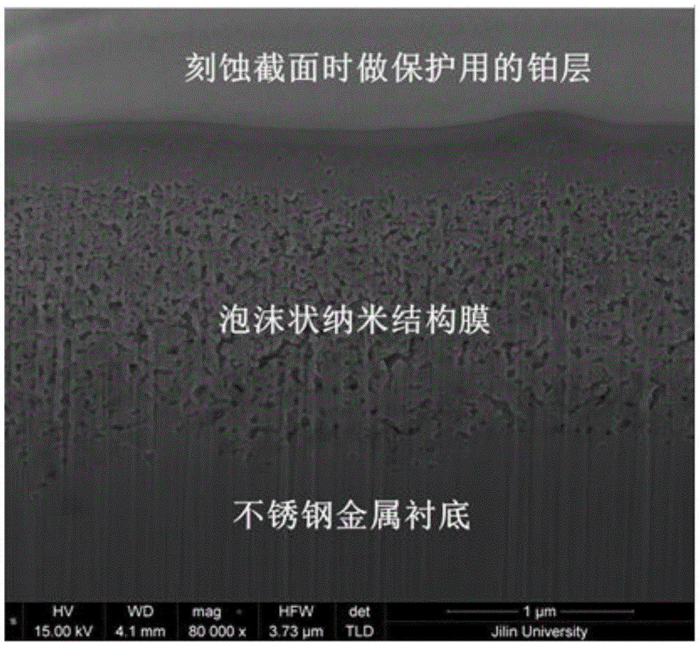
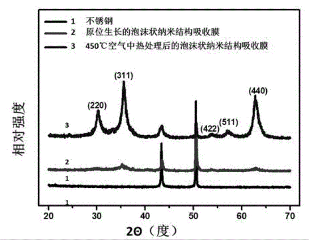
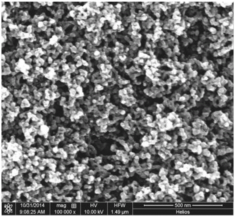
[0027] (2) Put the reaction kettle in an oven at 200 degrees Celsius for 22 hours, then take out the reaction kettle and cool it to room temperature naturally, and then ultrasonically treat it for 7 hours; finally take out the stainless steel sheet and wash it with deionized water, dry it at 90 degrees Celsius, and then A high-absorption and low-radiation solar spectrum selective absorption film with in-situ self-grown foam-like nanostructures is obtained on a stainless steel sheet. The thickness of the film is about 2.9 μm. There are relatively uniform pores accumulated in the film layer and on the surface of the film. The ...

Embodiment 2

[0033] Example 2: Preparation of stainless steel substrate / foamed nanostructured absorbing film

[0034] (1) First wipe the stainless steel sheet with alcohol cotton for 8 times to make the surface smooth and clean, then put it into 5M NaOH solution, and then pour it into the reaction kettle together.

[0035] (2) The reaction kettle was placed in an oven at 100°C for 6 hours, then the reaction kettle was taken out and cooled to room temperature naturally, the reaction product was subjected to ultrasonication for 7 hours, washed with deionized water, and dried at 20°C. The thickness of the film is about 1 μm. There are relatively uniform pores accumulated in the film layer and on the surface of the film. The particle size of the nanoparticle cluster is 35-59nm, and the size of the pores is 49-80nm. Depend on Figure 4 .2 The integral area ratio of the peaks of each element in the electron energy spectrum can be used to obtain the molar content ratio of each element on the fil...

Embodiment 3

[0036] Example 3: Preparation of stainless steel substrate / foamed nanostructured absorbing film

[0037] (1) First wipe the stainless steel sheet with alcohol cotton for 20 times to make the surface smooth and clean, then put it into 20M NaOH solution, and then pour it into the reaction kettle together.

[0038] (2) The reaction kettle was placed in an oven at 250 degrees Celsius for 40 hours, then the reaction kettle was taken out and cooled to room temperature naturally, the reaction product was subjected to ultrasonication for 25 hours, washed with deionized water, and dried at 90 degrees Celsius. The thickness of the film is about 3 μm. There are relatively uniform pores accumulated in the film layer and on the surface of the film. The particle size of the nanoparticle cluster is 20-44nm, and the size of the pores is 20-70nm. Depend on Figure 4 .3 The integral area ratio of the peaks of each element in the electron energy spectrogram can be used to obtain the molar conte...


PUM

PropertyMeasurementUnit
thicknessaaaaaaaaaa
particle diameteraaaaaaaaaa
sizeaaaaaaaaaa

Abstract

The invention provides an in-situ self-assembly growth solar selective absorbing film and a preparation method thereof, and belongs to the technical field of preparation of solar selective absorbing films. The in-situ self-assembly growth solar selective absorbing film consists of a stainless steel metal substrate and an in-situ self-assembly growth foamed nano-structure absorbing film body on the stainless steel metal substrate, wherein the thickness of the absorbing film body is 1-3 micrometers; and uniform holes formed by accumulated Fe3-x-yCrxNiyO4 of a spinal-type structure are distributed in a film layer and on a film surface, x equals to 0.18-0.27, y equals to 0.25-0.35, the grain size of nanometer particle clusters is 20-60 nanometers, and the size of the holes is 20-80 nanometers. On the premise that the absorbing film has high solar absorptivity and low heat emissivity, the in-situ self-assembly growth solar selective absorbing film is simple in structure, the foamed nano-structure grows on the substrate in an in-situ manner and is combined to the substrate closely and firmly, and heat stability and the weather resistance are high. The in-situ self-assembly growth solar selective absorbing film can be used in the field of solar photo-thermal generation heat collecting tubes.

Description

technical field [0001] The invention belongs to the technical field of preparation of solar spectrum selective absorption films, in particular to an in-situ self-grown foamy nanostructure high-absorption and low-radiation solar spectrum selective absorption film and a preparation method thereof. Background technique [0002] Solar thermal conversion is a kind of solar energy utilization method with high energy conversion efficiency and utilization rate and low cost, which can be widely promoted in the whole society. At present, solar thermal utilization is active and has formed an industry. Whether it is a solar water heater or a solar thermal power generation heat collector, there must be a core device for absorbing solar radiation, that is, a solar spectrum selective absorption coating. The coating is required to have a higher absorption rate in the visible-near infrared band (0.3-2.5 μm), and a lower emissivity in the infrared band (2.5 μm-20 μm). For a heated body in p...

Claims


Application Information

Patent Timeline
Patent Type & Authority Patents(China)
IPC IPC(8): F24J2/48
CPCF24S70/225Y02E10/40
Inventor 冯守华王兴利吴小峰黄科科
Owner JILIN UNIV
Learn More