

Back-passivation efficient PERL battery technology
A process and battery technology, applied in the field of high-efficiency PERL battery technology with back passivation, can solve the problems of unstable process, difficult removal of borosilicate glass phase, cross-doping, etc., and achieve the goal of simplifying the process flow, reducing production costs and reducing dosage Effect
- Summary
- Abstract
- Description
- Claims
- Application Information
AI Technical Summary
Problems solved by technology
Method used
Image

Examples
Embodiment 1
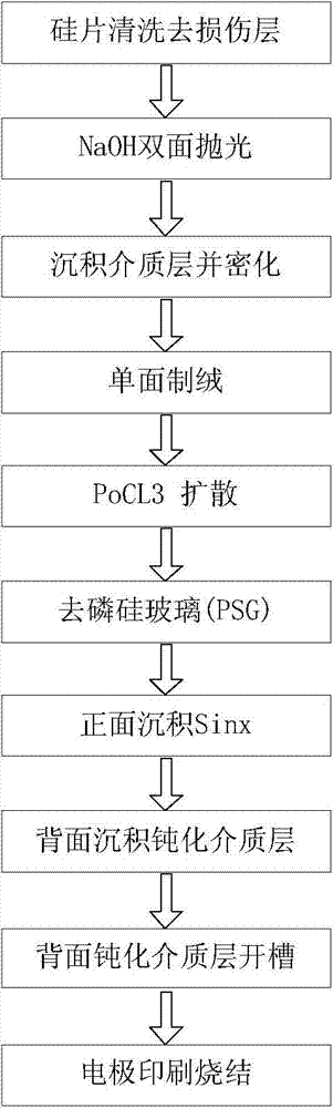
[0030] A back passivation high-efficiency PERL battery process, the process is as follows figure 1 As shown, the following steps are taken:
[0031] Step 1: Clean the original silicon wafer in HF / HNO3 mixed solution to remove surface damage layer, cutting line marks, etc.;
[0032] Step 2: Polishing the silicon wafer on both sides in NaOH solution;
[0033] Step 3: Deposit SiOx on one side of the polished silicon wafer. High-temperature thermal oxidation, PECVD or APCVD can be used to deposit SiOx film on one side, and anneal at 400°C to densify it;
[0034] Step 4: prepare a 1-2um high pyramid suede surface on one side of the above silicon wafer in TMAH;
[0035] Step 5: Deposit and diffuse POCL3 on one side of the above-mentioned silicon wafer in a high-temperature furnace;
[0036] Step 6: Using wet etching equipment to remove the surface phosphosilicate glass (PSG);
[0037] Step 7: Deposit SiNx with a thickness of about 80nm on the front side in a tube or plate PECVD ...
Embodiment 2
[0045] A back passivation high-efficiency PERL battery process, the process is the same as in embodiment 1, the difference is that step (3) deposits a SiNx dielectric layer on one side of the polished silicon wafer. Step (8) Depositing a SiOx dielectric layer on the back of the polished surface of the silicon wafer.
Embodiment 3
[0047] A back passivation high-efficiency PERL battery process, the process is the same as in embodiment 1, the difference is that step (3) deposits an a-Si dielectric layer on one side of the polished silicon wafer. Step (8) Depositing an a-Si dielectric layer on the back of the polished surface of the silicon wafer.
PUM
 Abstract
Description
Claims
Application Information