Layer-shaped high thermal conductive and insulating base plate and preparation method thereof
An insulating substrate, high thermal conductivity technology, applied in the field of electronics, can solve the problems of not having high-strength electrical insulation properties, low thermal conductivity of insulating materials, and inability to meet the high thermal conductivity of substrates, etc., to achieve good dimensional stability, low thermal expansion coefficient, high intensity effect
- Summary
- Abstract
- Description
- Claims
- Application Information
AI Technical Summary
Problems solved by technology
Method used
Image

Examples
Embodiment 1
[0023] The preparation method of the high thermal conductivity insulating substrate comprises the following steps:
[0024] Step 1: Prepare the diamond / copper composite material sample by pressure infiltration method. The volume fraction of diamond particles is 60%, and it is processed into a rectangular block of 30mm×40mm×3mm. Generally speaking, the shape of the composite material sample is Not set, and not limited to any thickness, but 2mm or more is the preferred thickness;
[0025] Step 2: Coarse grinding, fine grinding, rough polishing, and fine polishing of the diamond / copper composite material sample;
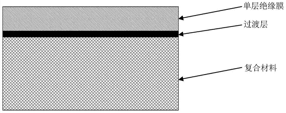
[0026] Step 3: Depositing a Ti transition layer on the diamond / copper composite material sample by magnetron sputtering, the thickness of the transition layer is 100nm;
[0027] Step 4: Deposit an AlN insulating film on the diamond / copper composite material sample deposited with a Ti transition layer by magnetron sputtering. The thickness of the insulating film is 3 μm...
Embodiment 2
[0029] The preparation method of the high thermal conductivity insulating substrate comprises the following steps:
[0030] Step 1: Prepare a diamond / copper composite material sample by pressure infiltration method, the volume fraction of diamond particles is 65%, and process it into a rectangular block of 40mm×50mm×3mm;
[0031] Step 2: Coarse grinding, fine grinding, rough polishing, and fine polishing of the diamond / copper composite material sample;
[0032] Step 3: Depositing a Ti transition layer on the diamond / copper composite material sample by magnetron sputtering, the thickness of the transition layer is 200nm;
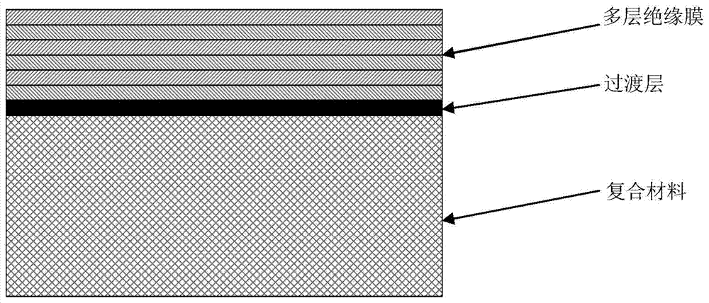
[0033] Step 4: Deposit an AlN insulating film on the diamond / copper composite material sample deposited with a Ti transition layer by magnetron sputtering, the thickness of the insulating film is 4 μm, and the dielectric strength of the diamond / copper composite substrate after depositing the AlN insulating film The electrical constant is 10.2, and the dielec...
Embodiment 3
[0035] The preparation method of the high thermal conductivity insulating substrate comprises the following steps:
[0036] Step 1: Prepare a diamond / aluminum composite material sample by pressure infiltration method, the volume fraction of diamond particles is 60%, and process it into a rectangular block of 35mm×45mm×3mm;
[0037] Step 2: Coarse grinding, fine grinding, rough polishing, and fine polishing of the diamond / aluminum composite material sample;
[0038] Step 3: Depositing a Ti transition layer on the diamond / aluminum composite material sample by magnetron sputtering, the thickness of the transition layer is 150nm;
[0039] Step 4: Deposit a BN insulating film on the diamond / aluminum composite material sample deposited with a Ti transition layer by magnetron sputtering. The thickness of the insulating film is 3 μm. After depositing the BN insulating film, the dielectric strength of the diamond / copper composite substrate The electrical constant is 4.5, and the diele...
PUM
| Property | Measurement | Unit |
|---|---|---|
| Thickness | aaaaa | aaaaa |
| Thickness | aaaaa | aaaaa |
| Thickness | aaaaa | aaaaa |
Abstract
Description
Claims
Application Information
 - Generate Ideas
- Intellectual Property
- Life Sciences
- Materials
- Tech Scout
- Unparalleled Data Quality
- Higher Quality Content
- 60% Fewer Hallucinations
Browse by: Latest US Patents, China's latest patents, Technical Efficacy Thesaurus, Application Domain, Technology Topic, Popular Technical Reports.
© 2025 PatSnap. All rights reserved.Legal|Privacy policy|Modern Slavery Act Transparency Statement|Sitemap|About US| Contact US: help@patsnap.com