Organic light-emitting device and preparation method thereof

An electroluminescent device and luminescence technology, which is applied in the direction of electric solid-state devices, semiconductor/solid-state device manufacturing, electrical components, etc., can solve the problems of low recombination probability of excitons and low luminous efficiency of devices, so as to improve electron injection efficiency and Electron transmission rate, improved light extraction efficiency, and high stability

Inactive Publication Date: 2015-06-24
OCEANS KING LIGHTING SCI&TECH CO LTD +2
View PDF0 Cites 0 Cited by
  • Summary
  • Abstract
  • Description
  • Claims
  • Application Information

AI Technical Summary

Problems solved by technology

[0004] In traditional organic electroluminescent devices, the electron transport rate is two or three orders of magnitude lower than the hole transport rate. Therefore, it is very easy to cause a low probability of exciton recombination, and the area where the excitons are recombined is not in the light-emitting area. Thereby reducing the luminous efficiency of the device

Method used


Image

  • Organic light-emitting device and preparation method thereof
  • Organic light-emitting device and preparation method thereof

Examples


Embodiment 1

[0043] A method for preparing an organic electroluminescent device, comprising the following steps:

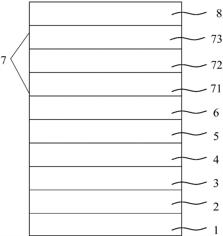
[0044] (1) Sonicate commercially available ordinary glass with detergent, deionized water, acetone, ethanol, and isopropanol for 15 minutes each to remove organic pollutants on the glass surface, clean it and air dry it; then use it on the glass substrate ITO with a thickness of 120nm was prepared by magnetron sputtering. The acceleration voltage of magnetron sputtering was 700V, the magnetic field was 120G, and the power density was 25W / cm 2 ; Then adopt the method of thermal resistance evaporation on the anode to prepare hole injection layer, hole transport layer, light-emitting layer and electron transport layer successively; Wherein,

[0045] The hole injection layer is made of MoO 3 , the pressure used in evaporation is 8×10 -4 Pa, the evaporation rate is 2nm / s, and the evaporation thickness is 40nm;

[0046] The material of the hole transport layer is NPB, and the pre...

Embodiment 2

[0057] A method for preparing an organic electroluminescent device, comprising the following steps:

[0058] (1) Sonicate commercially available ordinary glass with detergent, deionized water, acetone, ethanol, and isopropanol for 15 minutes each to remove organic pollutants on the glass surface, clean it and air dry it; then use it on the glass substrate AZO with a thickness of 300nm was prepared by magnetron sputtering. The acceleration voltage of magnetron sputtering was 300V, the magnetic field was 50G, and the power density was 40W / cm 2 ; Then adopt the method of thermal resistance evaporation on the anode to prepare hole injection layer, hole transport layer, light-emitting layer and electron transport layer successively; Wherein,

[0059] The material of the hole injection layer is V 2 o 5 , the pressure used in evaporation is 2×10 -3 Pa, the evaporation rate is 10nm / s, and the evaporation thickness is 20nm;

[0060] The material of the hole transport layer is TAPC,...

Embodiment 3

[0071] A method for preparing an organic electroluminescent device, comprising the following steps:

[0072] (1) Sonicate commercially available ordinary glass with detergent, deionized water, acetone, ethanol, and isopropanol for 15 minutes to remove organic pollutants on the glass surface, clean it and air dry it; then use it on the glass substrate AZO with a thickness of 150nm was prepared by magnetron sputtering. The acceleration voltage of magnetron sputtering was 800V, the magnetic field was 200G, and the power density was 1W / cm 2 ; Then adopt the method of thermal resistance evaporation on the anode to prepare hole injection layer, hole transport layer, light-emitting layer and electron transport layer successively; Wherein,

[0073] The material of the hole injection layer is V 2 o 5 , the pressure used in evaporation is 5×10 -5 Pa, the evaporation rate is 1nm / s, and the evaporation thickness is 55nm;

[0074] The material of the hole transport layer is TCTA, and the...


PUM

PropertyMeasurementUnit
Thicknessaaaaaaaaaa
Thicknessaaaaaaaaaa
Thicknessaaaaaaaaaa

Abstract

The invention discloses an organic light-emitting device and a preparation method thereof. The organic light-emitting device comprises a glass substrate, a conductive anode, a hole injection layer, a hole transport layer, a light-emitting layer, an electron transport layer, electron injection layers and a cathode which are sequentially overlapped. The electron injection layers include the fullerene derivate layer, the thiophene compound layer and the metal oxide layer which are sequentially overlapped. The fullerene derivate layer is arranged on the surface of the electron transport layer. The fullerene derivate layer is made of footballene or carbon 70 or [6,6]-phenyl-C61-butyric acid methyl ester or [6,6]-phenyl-C71-butyric acid methyl ester. The thiophene compound layer is made of 3-hexylthipphene or 3-methylthiophene or 3-octylthiophene or 3-dodecylthiophene. The metal oxide layer is made of molybdenum trioxide or tungsten trioxide or vanadium pentoxide. By means of the electron injection layers, the light-emitting efficiency of the device can be effectively improved.

Description

technical field [0001] The invention relates to the field of organic electroluminescence, in particular to an organic electroluminescence device and a preparation method thereof. Background technique [0002] In 1987, C.W.Tang and Van Slyke of Eastman Kodak Company in the United States reported a breakthrough in the research of organic electroluminescence. A high-brightness, high-efficiency double-layer organic electroluminescent device (OLED) has been prepared using ultra-thin film technology. Brightness up to 1000cd / m at 10V 2 , its luminous efficiency is 1.51lm / W, and its lifespan is more than 100 hours. [0003] The principle of OLED light emission is based on the action of an external electric field, electrons are injected from the cathode to the lowest unoccupied molecular orbital (LUMO) of organic matter, and holes are injected from the anode to the highest occupied orbital (HOMO) of organic matter. Electrons and holes meet, recombine, and form excitons in the ligh...

Claims


Application Information

Patent Timeline
IPC IPC(8): H01L51/50H01L51/54H01L51/56H01L51/52
Inventor 周明杰黄辉陈吉星王平
Owner OCEANS KING LIGHTING SCI&TECH CO LTD
Why Eureka
Try Eureka