Optical transceiver with serial-parallel conversion function

A technology for optical transceivers and conversion functions, which is applied in the field of optical transceivers, and can solve the problems of restricting processor chip interface bandwidth, limiting communication carriers, and large power consumption.

Active Publication Date: 2015-06-24
NAT UNIV OF DEFENSE TECH
View PDF6 Cites 16 Cited by
  • Summary
  • Abstract
  • Description
  • Claims
  • Application Information

AI Technical Summary

Problems solved by technology

Due to the use of two-stage indirect conversion and the need for high-speed serial electrical signals as a transition, this brings many limitations to traditional solutions
First of all, although the optical interconnection technology has the advantage of low power consumption, the traditional solution continues to use the high-power SerDes circuit, so that the power consumption in the transmission process is still very large, and the single-channel 25Gbps EDR (Enhanced Data Rate, enhanced rate) technology as an example, the power consumption of SerDes circuits has accounted for more than 75% of the total power consumption of node input and output chips, and this ratio is as high as more than 90% for routing chips
Secondly, although the theoretical rate of a single channel of optical

Method used


Image

  • Optical transceiver with serial-parallel conversion function
  • Optical transceiver with serial-parallel conversion function
  • Optical transceiver with serial-parallel conversion function

Examples


Embodiment Construction

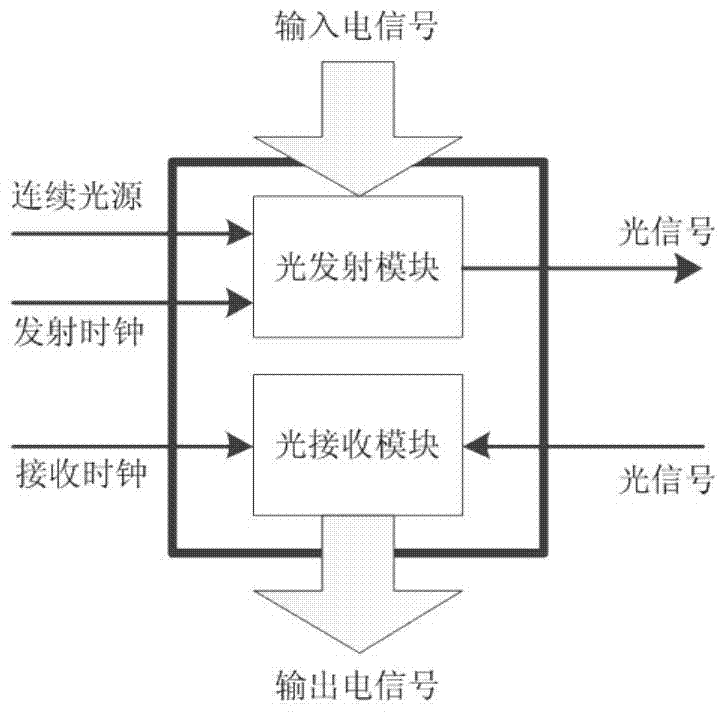
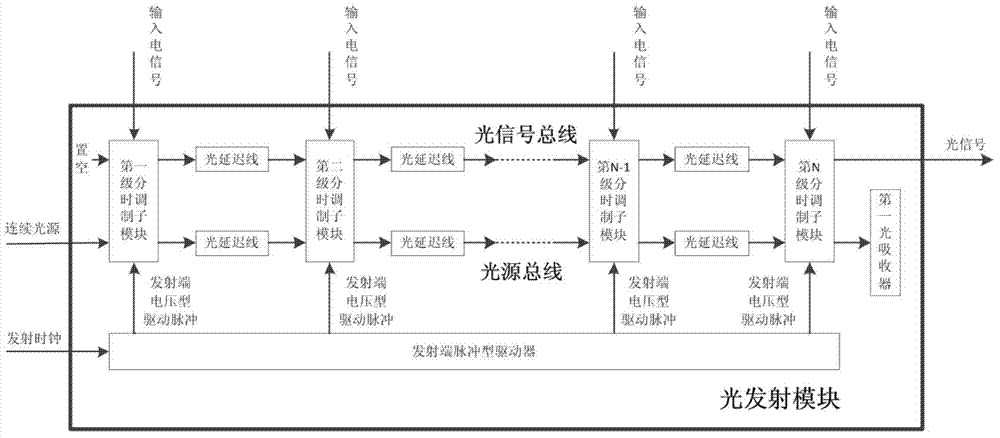
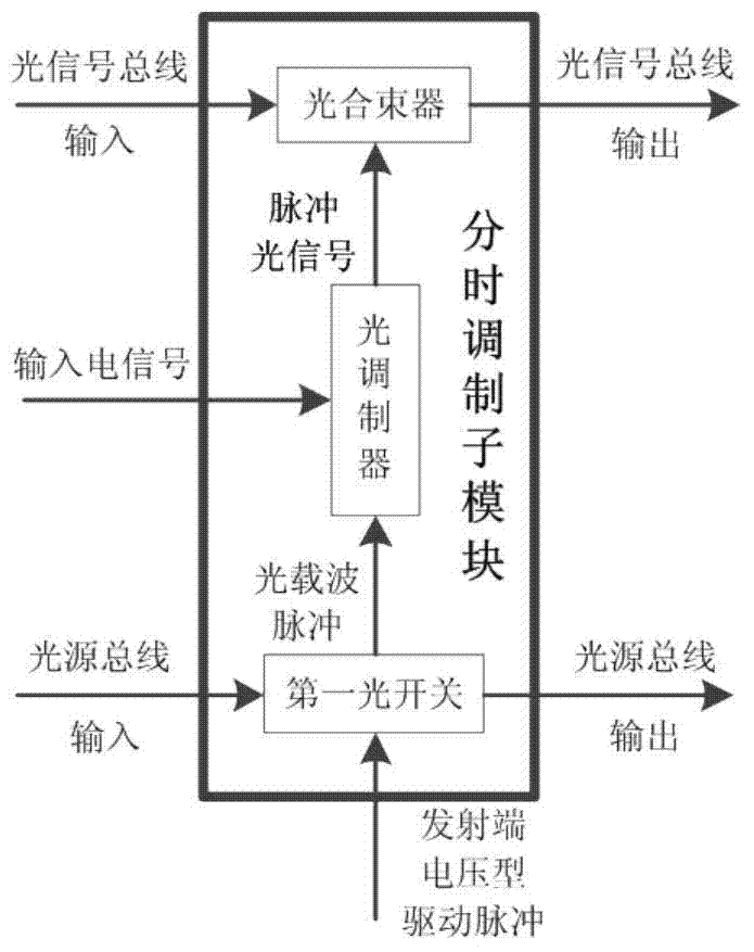
[0024] The following is an example of a 20-fold frequency optical transceiver with a main frequency of 2.5GHz, i.e. f=2.5GHz, τ=20ps, N=20, the optical transceiver containing the serial-to-parallel conversion function of the present embodiment is described, wherein the numbers are all from 0 to start.

[0025] 1. The main frequency of the optical transceiver is 2.5GHz, the transmit clock and receive clock frequency is 2.5GHz, and one beat is 400ps. The frequencies of the input electrical signal and the output electrical signal are also 2.5 GHz, the input electrical signal is aligned with the rising edge of the transmitting clock, and the output electrical signal is aligned with the rising edge of the receiving clock. The optical serial signal output by the optical transceiver is 20 times the main frequency of 2.5GHz, that is, 50GHz.

[0026] 2. The optical carrier adopts 1550nm infrared light, which is provided by an off-chip distributed feedback Bragg grating (DFB) laser, an...


PUM

PropertyMeasurementUnit
Amplitudeaaaaaaaaaa

Abstract

The invention discloses an optical transceiver with a serial-parallel conversion function, and aims at providing a device which can switch a low-speed parallel electric signal and a high-speed serial optical signal. The optical transceiver is composed of a light emitting module and a light receiving module. The light emitting module is composed of N stages of time-sharing modulation submodules, a transmitting terminal pulse type driver and a first light absorption device. Each stage of time-sharing modulation submodule is composed of a first optical switch, a light modulator and a light beam combination device. The light receiving module is composed N stages of time-sharing demodulation submodules, a parallel shaping amplifier array, a receiving end pulse type driver and a second light absorption device, wherein the N stages of time-sharing demodulation submodules are connected to an optical signal bus in series through light delay lines. Each stage of time-sharing demodulation submodule is composed of a second optical switch and a light detector. By means of the optical transceiver, serial-parallel conversion can be conducted on a light path while photovoltaic conversion is conducted, the link serial rate is increased, the bandwidth of a processor chip interface is increased, the power consumption in the information transmission process is lowered, and the signal quality of communication links is improved.

Description

Technical field: [0001] The invention relates to a photoelectric conversion technology and a serial-to-parallel conversion technology in an optical interface of a chip, in particular to an optical transceiver, which can realize a serial-to-parallel conversion function while completing photoelectric conversion. Background technique: [0002] As the computing speed of high-performance computers continues to increase from petascale to petascale, the ability of microprocessor chips to process information is greatly improved, and the amount of data exchange between computing nodes in high-performance computer systems increases exponentially. The demand for interconnection network interface bandwidth continues to increase. On the other hand, VLSI technology is increasingly approaching its physical limit, especially in the interconnection and communication between processor chips and processor chips of high-performance computers, and between processor chips and high-speed memory ch...

Claims


Application Information

Patent Timeline
IPC IPC(8): H04B10/40H04B10/524H04B10/61
Inventor 罗章王克非徐炜遐庞征斌陆平静夏军赖明澈张建民
Owner NAT UNIV OF DEFENSE TECH
Why Eureka
Try Eureka