Nickel-chromium plating part and manufacturing method thereof
A manufacturing method and component technology, applied in nickel-chrome-plated components and its manufacturing field, can solve problems such as poor corrosion resistance, corrosion resistance that cannot meet the requirements of corrosive environments, and unsuitable products
- Summary
- Abstract
- Description
- Claims
- Application Information
AI Technical Summary
Problems solved by technology
Method used
Image
Examples
Embodiment 1
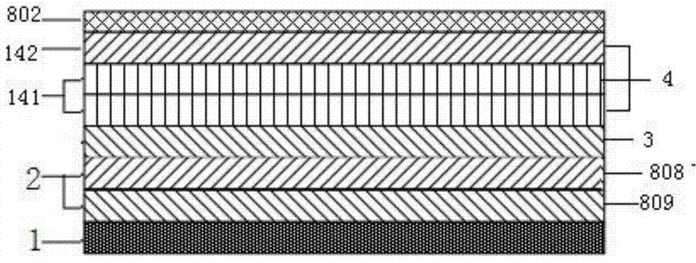
[0080] The nickel-chromium plating part of the present embodiment, this part comprises: base material 1 (ABS material); Pretreatment plating layer 2 comprises chemical nickel layer 809, makes a bottom nickel layer 808 and copper-plated layer 3, and chemical nickel layer deposits 809 to deposit on On the whole substrate 1, a bottoming nickel layer 808 is deposited on the chemical nickel layer 809, and a copper plating layer 3 is formed on the bottoming nickel layer 808; and a functional layer 4, which is formed on the copper plating layer 3, wherein the functional layer 4 comprising a low-potential nickel layer 141 and a microporous nickel layer 142, wherein the low-potential nickel layer 141 is a high-sulfur nickel layer, the microporous nickel layer 142 formed on the high-sulfur nickel layer; and the microporous nickel layer 142 formed on the microporous nickel layer 142 Decorative layer 802 (trivalent white chrome plating).
Embodiment 2
[0082] The nickel-chromium plating part of the present embodiment, this part comprises: base material 1 (ABS material); Pretreatment plating layer 2 comprises chemical nickel layer 809, makes a bottom nickel layer 808 and copper-plated layer 3, and chemical nickel layer deposits 809 to deposit on On the whole substrate 1, a bottoming nickel layer 808 is deposited on the chemical nickel layer 809, and a copper plating layer 3 is formed on the bottoming nickel layer 808; and a functional layer 4, which is formed on the copper plating layer 3, wherein the functional layer 4 comprising a low-potential nickel layer 141 and a microporous nickel layer 142, wherein the low-potential nickel layer 141 is a microcracked nickel layer, the microporous nickel layer 142 formed on the microcracked nickel layer; and the microporous nickel layer 142 formed on the microporous nickel layer 142 Decorative layer 802 (trivalent black chrome plating).
Embodiment 3
[0084] The nickel-chromium plating part of the present embodiment, this part comprises: base material 1 (ABS material); Pretreatment plating layer 2 comprises chemical nickel layer 809, makes a bottom nickel layer 808 and copper-plated layer 3, and chemical nickel layer deposits 809 to deposit on On the whole substrate 1, a bottoming nickel layer 808 is deposited on the chemical nickel layer 809, and a copper plating layer 3 is formed on the bottoming nickel layer 808; and a functional layer 4, which is formed on the copper plating layer 3, wherein the functional layer 4 includes a low-potential nickel layer 141 and a microporous nickel layer 142, wherein the low-potential nickel layer 141 is a high-sulfur nickel layer and a micro-crack nickel layer (it may be that the high-sulfur nickel layer is formed on the copper plating layer 3, and the micro-crack nickel layer is formed On the high-sulfur nickel layer; it can also be that the micro-crack nickel layer is formed on the copp...
PUM
 Abstract
Description
Claims
Application Information


