Surface-enhanced Raman spectroscopy substrate and preparation method thereof

A surface-enhanced Raman and substrate technology, applied in the field of spectral analysis, to achieve the effects of expanding the use and industrialization prospects, increasing the electric field intensity, and enhancing the electric field

Active Publication Date: 2015-07-22
JIANGSU UNIV OF TECH
View PDF4 Cites 21 Cited by
  • Summary
  • Abstract
  • Description
  • Claims
  • Application Information

AI Technical Summary

Problems solved by technology

[0006] However, the existing technologies using gold nanostar particles as Raman gain medium often only use the electric field enhancement characteristics of nanostars themselves

Method used


Image

  • Surface-enhanced Raman spectroscopy substrate and preparation method thereof
  • Surface-enhanced Raman spectroscopy substrate and preparation method thereof
  • Surface-enhanced Raman spectroscopy substrate and preparation method thereof

Examples


Embodiment 1

[0040] (Example 1, Surface Enhanced Raman Scattering Substrate)

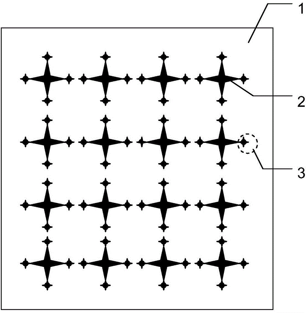
[0041] See figure 1 , the surface-enhanced Raman scattering substrate of this embodiment includes a conductive substrate 1, a two-dimensional noble metal micro-nanostructure array 2 and gold nanostars 3, and the two-dimensional noble metal micro-nanostructure array 2 and gold nanostars 3 are located on the conductive substrate 1 on one side surface.

[0042] The conductive substrate 1 is conductive glass or silicon wafer.

[0043] The two-dimensional noble metal micro-nano structure array 2 is composed of array units aligned vertically and laterally. Each array unit is a star-shaped noble metal thin film, and the noble metal thin film is a gold thin film, a silver thin film or a platinum thin film. The size of each star-shaped noble metal thin film unit is 150nm-1000nm, and the distance between two adjacent units is 10nm-500nm. The array unit is three-pointed star, four-pointed star, five-pointed star, six-po...

Embodiment 2

[0045] (Example 2, preparation method of surface-enhanced Raman scattering substrate)

[0046] In this example, the surface-enhanced Raman scattering substrate described in Example 1 is prepared, and the preparation method includes the following steps:

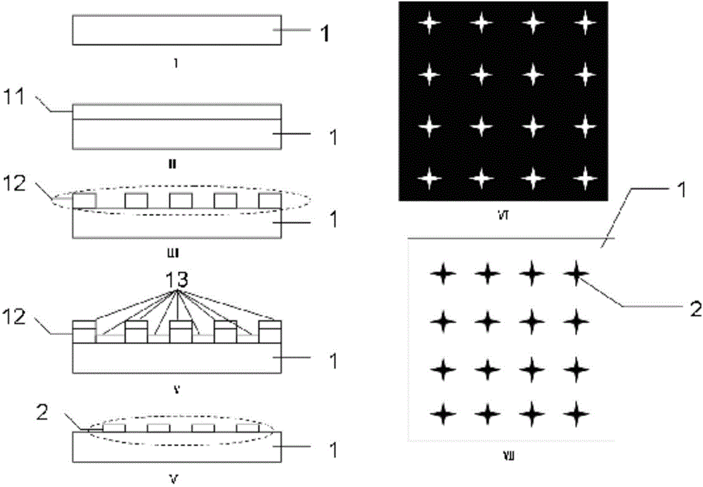
[0047] ① A photoresist layer containing a two-dimensional star-shaped micro-nano structure array pattern is prepared on the conductive substrate 1 .

[0048] See figure 2 I. First, the conductive substrate 1 is cleaned to remove particles and impurity ions on the surface. When cleaning, use detergent, acetone, and isopropanol to clean in sequence, and dry them after cleaning.

[0049] See figure 2 II. Spin-coat a layer of positive photoresist 11 on the dried conductive substrate 1, and the thickness of the photoresist 11 is 200nm-500nm.

[0050] See figure 2 III. Soft-baking the photoresist 11 with a hot plate, the temperature of the hot plate is 85°C-120°C, and the soft-baking time is 30s-60s. After the soft baking i...


PUM

PropertyMeasurementUnit
sizeaaaaaaaaaa
particle diameteraaaaaaaaaa

Abstract

The invention discloses a surface-enhanced Raman spectroscopy substrate and a preparation method thereof. The surface-enhanced Raman spectroscopy substrate comprises a conducting substrate, a two-dimensional noble metal micro-nano structure array and gold nanostars, wherein each array unit is a starlike noble metal film unit; the size of each starlike noble metal film unit is 150-1000 nm; the distance between every two adjacent starlike noble metal film units is 10-500 nm; the gold nanostars are deposited at tips of all the starlike noble metal film units in the two-dimensional noble metal micro-nano structure array through electrophoresis; the deposition position of each gold nanostar is 1-5 nm away from the tips of the corresponding starlike noble metal film unit. On one hand, the own electric fields of gold nanostar particles are enhanced; on the other hand, the tips of all the starlike noble metal film units in the two-dimensional noble metal micro-nano structure array are further coupled with those of the gold nanostar particles. Therefore, the electric field strength in a nearby area is greatly improved, and the high-sensitivity surface-enhanced Raman spectroscopy substrate is obtained.

Description

technical field [0001] The invention relates to spectral analysis technology, in particular to a surface-enhanced Raman scattering substrate and a preparation method thereof. Background technique [0002] Raman spectroscopy can be widely used in the field of molecular recognition, but ordinary Raman scattering signals are weak and difficult to detect, which limits its practical application. Surface enhanced Raman scattering (SERS) spectroscopy technology greatly enhances the ordinary Raman signal by constructing a special surface substrate, so as to effectively detect low-concentration molecules and become an important tool for the detection of trace molecules of substances . [0003] In recent years, noble metal nanomaterials have aroused widespread interest in the field of nanotechnology due to their unique optical, electrical, mechanical, catalytic and biocompatibility properties, especially in the material analysis and inspection technology based on surface-enhanced Ram...

Claims


Application Information

Patent Timeline
Patent Type & Authority Applications(China)
IPC IPC(8): G01N21/65C03C17/36C04B41/52C25D15/00
CPCC03C17/10C03C17/3649C03C17/40C04B41/5116C04B41/52G01N21/658C04B41/51
Inventor 朱圣清周健杨润苗周仕龙
Owner JIANGSU UNIV OF TECH
Why Eureka
Try Eureka