Method for growing graphene in silicon micro-channel plate

A silicon microchannel plate and graphene technology, applied in the field of microelectromechanical systems, can solve the problems of expensive equipment, difficult process, difficult industrialization, etc., and achieve the effects of low cost, avoiding complex processes and being environmentally friendly

Inactive Publication Date: 2015-08-12
EAST CHINA NORMAL UNIVERSITY
View PDF10 Cites 3 Cited by
  • Summary
  • Abstract
  • Description
  • Claims
  • Application Information

AI Technical Summary

Problems solved by technology

Among these methods, the redox method and the metal surface growth method are mostly used. The graphene prepared by the redox method has a high yield and is suitable for large-scale production. However, the graphene prepared by this method has many defects and can only be used in supercapacitors. , lithium-ion batteries and other en

Method used


Image

  • Method for growing graphene in silicon micro-channel plate
  • Method for growing graphene in silicon micro-channel plate
  • Method for growing graphene in silicon micro-channel plate

Examples


Example Embodiment

[0043] Example 1

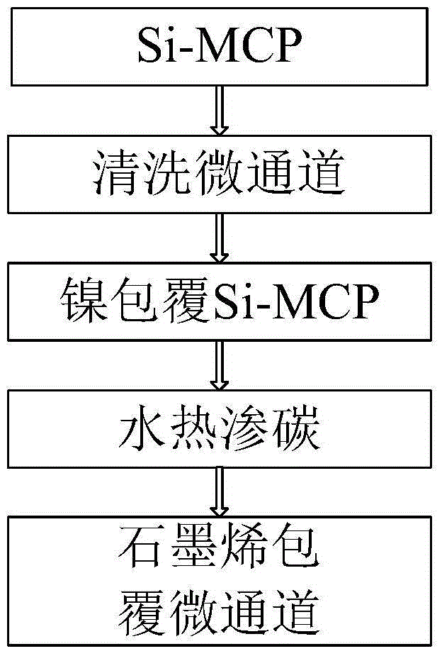
[0044] One method of growing graphene in a microchannel plate is as follows:

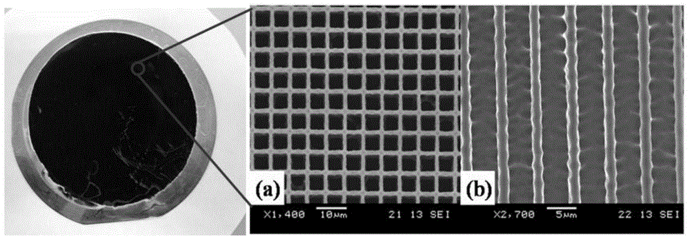
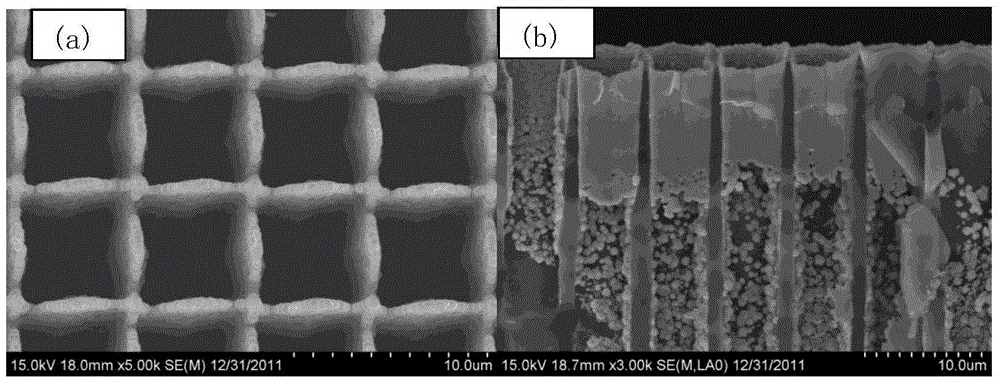
[0045] 1. Choose a silicon microchannel plate made of p-type silicon with (100) crystal orientation, the aperture size is 5×5×250, the unit is micron, the aspect ratio is 50, and the area is 1×1, and the unit is centimeter, such as figure 1 shown;

[0046] 2. Take 50ml of corrosion solution as HF:C2H5OH:H2O=100:125:10 volume ratio, soak the silicon microchannel plate for 3 minutes, and remove the silicon dioxide naturally grown on the surface of the silicon microchannel;

[0047] 3. Soak the silica-removed silicon microchannel plate in a surfactant whose concentration is Triton-X100:H2O=1 / 500 volume ratio, and soak for 60 seconds. Improve the wettability of the silicon microchannel hole wall and surface, drive out the air in the silicon microchannel hole; configure the electroless nickel plating solution, the ratio of which is NiCl 2 :NH 4 Cl:NaH 2 PO 4 =5:5.1:1.2 (mass rati...

Example Embodiment

[0050] Example 2

[0051] 1. A method for growing graphene in a microchannel plate is as follows: select the silicon microchannel plate prepared by (100) crystalline p-type silicon, the aperture size is 5 × 5 × 250, the unit is micron, and the aspect ratio is 50, Area 1cm×1cm, such as figure 1 shown;

[0052] 2. Take 50ml corrosion solution as HF:C 2 h 5 OH:H2O=100:125:10 volume ratio, soak the silicon microchannel plate for 4 minutes to remove the silicon dioxide naturally grown on the surface of the silicon microchannel;

[0053] 3. Soak the silica-removed silicon microchannel plate in surfactant with a concentration of Triton-X100:H 2 O=1 / 1000 volume ratio, soak for 30 seconds. Improve the wettability of the wall and surface of the silicon microchannel, and drive out the air in the hole of the silicon microchannel;

[0054] 4. Configure the electroless nickel plating solution, the ratio of which is NiCl 2 :NH 4 Cl:NaH 2 PO 4 =5:5.1:1.2 (mass ratio), configure 100m...


PUM


Abstract

The invention discloses a method for growing graphene in a silicon micro-channel plate. The method comprises the following steps: (1) pretreatment: soaking the silicon micro-channel plate into corrosive liquid; (2) electroless nickel plating: putting the pretreated silicon micro-channel plate into an electroless nickel plating solution to perform chemical plating of porous nickel; (3) hydrothermal polyol carburization: soaking the nickel-plated silicon micro-channel plate into a surfactant once again, and putting the soaked nickel-plated silicon micro-channel plate into a hydrothermal reaction kettle filled with polyol and a sodium salt catalyst; and (4) annealing: annealing the silicon micro-channel plate containing nickel carbide in a tubular furnace. Compared with the prior art, the method has the advantages that the problem of failure in plugging graphene into a silicon micro-channel with an electrophoretic technique is solved; and meanwhile, the defects of complex graphene growing process and high cost in a chemical vapor deposition method are overcome. A plurality of layers of graphene can be grown on the surface and in holes of the nickel-plated silicon micro-channel plate with a high depth-width ratio. The method has the characteristics of environmental friendliness, easiness, feasibility, low cost and the like.

Description

technical field [0001] The invention belongs to the technical field of microelectromechanical systems, and in particular relates to a method for growing graphene in a silicon microchannel plate. Background technique [0002] Graphene was obtained by Andre Geim and Konstantin Novoselov of the University of Manchester in 2004 through the method of mechanical stripping of adhesive tape. In 2010, they won the Nobel Prize in Physics for this. Graphene is a two-dimensional crystal composed of carbon atoms. The thickness of a single layer is 0.335nm, which is 1 / 200 of the thickness of a hair. 1 mm thick graphite has 1.5 million layers of graphene, and the specific surface area of ​​graphene reaches 26002600m 2 / g. Graphene has excellent electrical conductivity, large specific surface area, tens of times stronger strength than steel, and good light transmission. It has broad applications in the fields of electronic devices, touch screens, biomedicine, sensors, super capacitors, and...

Claims


Application Information

Patent Timeline
IPC IPC(8): B81C1/00
Inventor 王连卫吴大军
Owner EAST CHINA NORMAL UNIVERSITY
Why Eureka
Try Eureka