III-nitride semiconductor/quantum dot hybrid white light LED device and preparing method thereof

A technology of nitride semiconductors and LED devices, which is applied in semiconductor devices, electrical components, circuits, etc., can solve the problems of low conversion efficiency and long-term decay of yellow fluorescent pink, and achieve the effect of overcoming rough surfaces and improving luminous efficiency

Active Publication Date: 2015-08-26
NANJING UNIV
View PDF6 Cites 28 Cited by
  • Summary
  • Abstract
  • Description
  • Claims
  • Application Information

AI Technical Summary

Problems solved by technology

However, the inevitable disadvantages of this phosphor solution include: self-absorption, long-term decay, low conversion efficiency of yellow phosphor pink
From the currently disclosed phosphor-f

Method used


Image

  • III-nitride semiconductor/quantum dot hybrid white light LED device and preparing method thereof
  • III-nitride semiconductor/quantum dot hybrid white light LED device and preparing method thereof
  • III-nitride semiconductor/quantum dot hybrid white light LED device and preparing method thereof

Examples


Embodiment 1

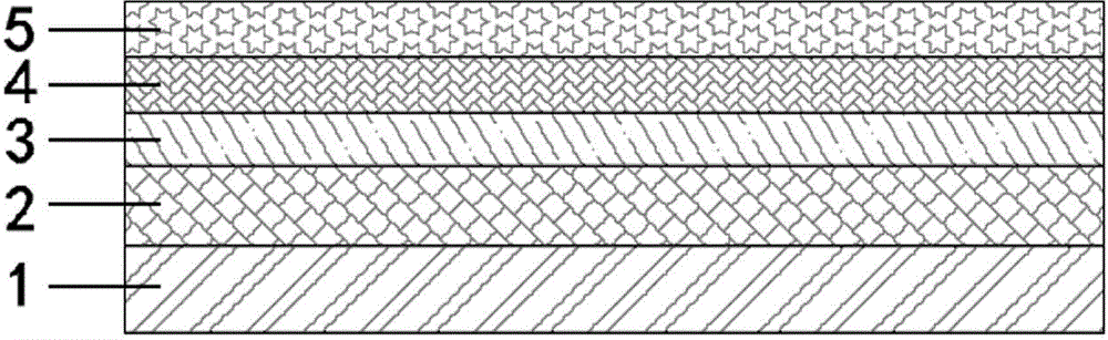
[0064] like Figure 1-11 Shown, the preparation method of this white light LED device, its step comprises:

[0065] 1) Select an InGaN / GaN quantum well LED substrate with x as 0.12, luminous wavelength as 430nm, period number of quantum well as 10, and thickness of p-type GaN as 300nm, and deposit a layer of ITO on it by electron beam evaporation technology , the thickness is 100nm, and then the sample is annealed at a high temperature in a rapid annealing furnace (RTA), the annealing temperature is 450°C, and the time is 2min;

[0066] 2) A layer of SiO was grown on the surface of the ITO layer by plasma-enhanced chemical vapor deposition 2 layer, with a thickness of 30 nm, was deposited on SiO by physical vapor deposition 2 A layer of Ni metal film layer is grown on the surface of the layer, the thickness is 10nm, and 200nm thick SU8 glue and 30nm thick UV curing glue are sequentially spin-coated on the surface of the Ni metal film layer;

[0067] 3) Using UV-NIL technolo...

Embodiment 2

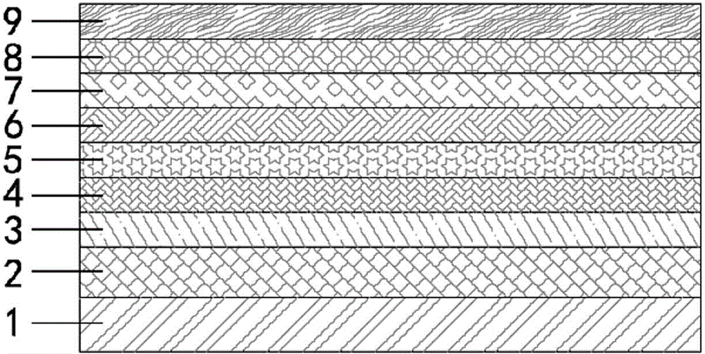
[0078] like Figure 1-11 Shown, the preparation method of this white light LED device, its step comprises:

[0079] 1) Choose an InGaN / GaN quantum well LED substrate with x as 0.25, luminous wavelength as 480nm, period number of quantum well as 15, and thickness of p-type GaN as 500nm, and deposit an ITO layer on it by electron beam evaporation technology , the thickness is 200nm, and then the sample is annealed at a high temperature in a rapid annealing furnace (RTA), the annealing temperature is 600°C, and the time is 10min;

[0080] 2) A layer of SiN is grown on the surface of the ITO layer by plasma-enhanced chemical vapor deposition x layer, with a thickness of 300nm, was deposited on Si by physical vapor deposition 3 N 4 A layer of Cr metal film layer is grown on the surface of the layer, and the thickness is 50nm. The SU8 glue with a thickness of 600nm and the UV curing glue with a thickness of 300nm are spin-coated on the surface of the Cr metal film layer in turn; ...

Embodiment 3

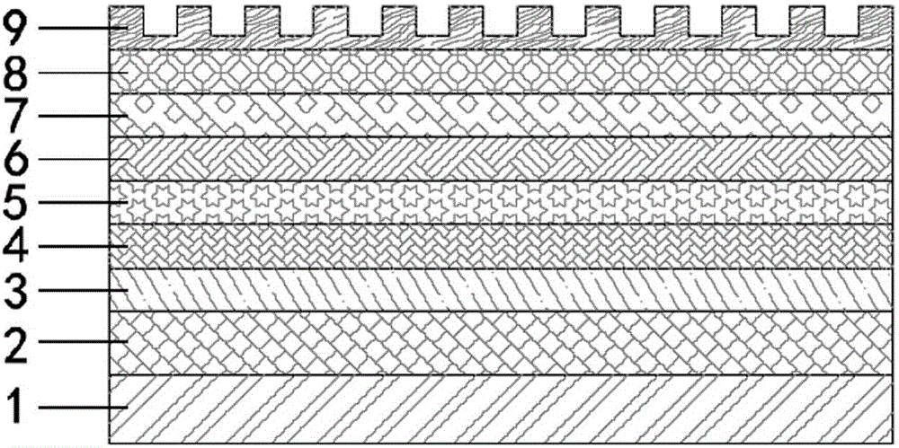
[0092] like Figure 1-11 Shown, the preparation method of this white light LED device, its step comprises:

[0093] 1) Choose an InGaN / GaN quantum well LED substrate with x as 0.18, luminous wavelength as 450nm, period number of quantum well as 12, and thickness of p-type GaN as 400nm, and deposit a layer of ITO on it by electron beam evaporation technology , the thickness is 150nm, and then the sample is annealed at a high temperature in a rapid annealing furnace (RTA), the annealing temperature is 500°C, and the time is 6min;

[0094] 2) A layer of SiN is grown on the surface of the ITO layer by plasma-enhanced chemical vapor deposition x layer, with a thickness of 160 nm, was deposited on Si by physical vapor deposition 3 N 4 A layer of Al metal film layer is grown on the surface of the layer, the thickness is 30nm, and 450nm thick SU8 glue and 160nm thick UV curing glue are sequentially spin-coated on the surface of the Al metal film layer;

[0095] 3) Using UV-NIL tec...


PUM

PropertyMeasurementUnit
Luminous wavelengthaaaaaaaaaa
Thicknessaaaaaaaaaa
Thicknessaaaaaaaaaa

Abstract

The invention discloses an III-nitride semiconductor/quantum dot hybrid white light LED device. According to the invention, an ordered nano-pore array is arranged outside the regions of a p type electrode and an n type electrode. The nano-pore array penetrates from the surface of the device through a quantum well active layer to the inner part of an n type nitride layer. The nano-pore array is internally filled with II-VI quantum dots. The invention further discloses a preparing method of the III-nitride semiconductor/quantum dot hybrid white light LED device. Non-radiative composite energy transferring between an indium gallium nitrogen (InGaN) quantum well and excitons in the II-VI quantum dots is utilized by the device to improved the light emitting efficiency of the device; in addition, by changing the types and the ratio of the filling quantum dots, the wavelength and the intensity of emitted light is adjusted, and the white light LED device with the nitride/quantum dot hybrid structure is capable of realizing a superhigh color rendering index.

Description

technical field [0001] The invention relates to a group III nitride semiconductor / quantum dot mixed white light LED device and a preparation method thereof, belonging to the field of semiconductor lighting. Background technique [0002] Group III nitride materials are direct bandgap semiconductors, and their bandgap covers from infrared to visible light to ultraviolet bands. They are ideal materials for solid-state lighting and low-power displays. Solid-state lighting is a brand-new lighting field. It mainly uses semiconductor chips as light sources to directly convert electrical energy into light energy with high conversion efficiency. As the core component of solid-state lighting semiconductor light source, LED has low energy consumption, long life, small size, green environmental protection, safe use, and can work in various harsh environments. It is a new generation of lighting source after incandescent lamps and fluorescent lamps. With the continuous development of lig...

Claims


Application Information

Patent Timeline
IPC IPC(8): H01L33/00H01L33/06
CPCH01L33/005H01L33/06
Inventor 刘斌张荣庄喆谢自力葛海雄郭旭陈鹏陈敦军韩平施毅郑有炓
Owner NANJING UNIV
Why Eureka
Try Eureka