Multi-waveguide integrated resonance semiconductor laser

A technology integrating resonance and semiconductor, applied in the field of new semiconductor lasers, can solve the problems of narrow linewidth, high beam quality, high coherence, etc., and achieve the effect of improving energy density, high brightness and good stability

Active Publication Date: 2015-09-09
吉光半导体科技有限公司
View PDF5 Cites 5 Cited by
  • Summary
  • Abstract
  • Description
  • Claims
  • Application Information

AI Technical Summary

Problems solved by technology

[0005] In order to solve the problems existing in the prior art, the present invention provides a multi-waveguide integrated resonant semiconductor laser, which mainly solves the problems of high power, high beam quality, high brightness, narrow line width and high coherence of semiconductor laser single tube and linear array The problem

Method used


Image

  • Multi-waveguide integrated resonance semiconductor laser
  • Multi-waveguide integrated resonance semiconductor laser
  • Multi-waveguide integrated resonance semiconductor laser

Examples


Embodiment 1

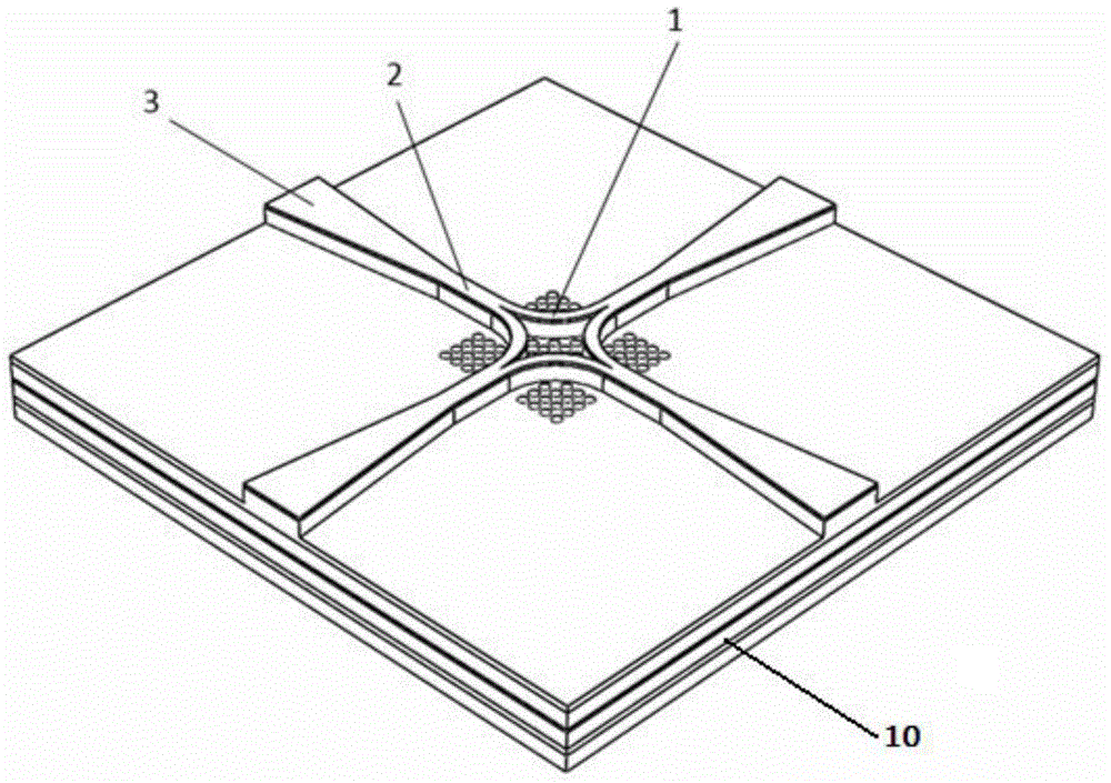
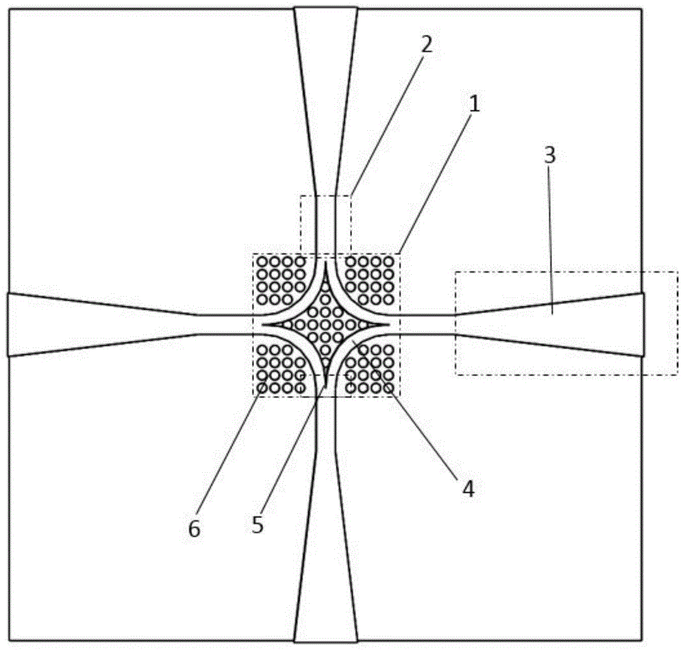
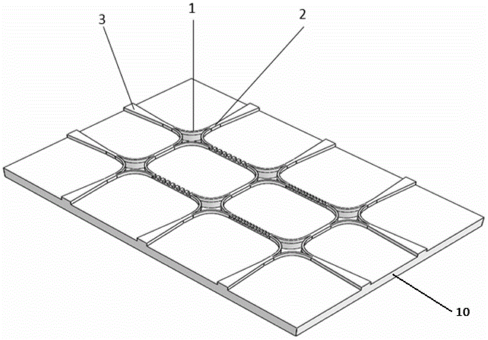
[0028] Such as figure 1 and figure 2 As shown, in this embodiment, on the designed and prepared semiconductor laser chip 10 with a wavelength of 980nm and an effective refractive index of 3.48 in this wavelength band, photonic bridge 1 is etched out at one time by photolithography and etching methods. , the mode stabilizer 2, and the ridge-shaped raised portion of the power amplifier 3. Then, the photonic crystal is further prepared downward on the lower mesa of the ridge by electron beam engraving. Among them, the specific size requirement of the photonic crystal is that the 980nm laser is within the photonic band gap of the photonic crystal, and the 980nm photons are not allowed to propagate in it; Shaped foot 88°. Then the usual semiconductor process is carried out, that is, evaporating oxide insulating layer, photolithography overlay electrode window, making metal electrode for ohmic contact, chip jointing, cavity surface coating and other processes. In this embodimen...

Embodiment 2

[0030] Such as image 3 and Figure 4 As shown, in this embodiment, on the semiconductor laser chip 10 that has been designed and prepared near the wavelength of 980nm and has an effective refractive index of 3.48 in this wavelength band, firstly, by photolithography or electron beam etching, the designed Position the grating structure in the mode stabilizer 2, in this embodiment, when the multi-waveguide integrated resonant semiconductor laser is designed to work at a single wavelength of 980nm, the period of the grating is 281.6nm; when the multi-waveguide integrated resonant semiconductor laser design wavelength is When the dual-wavelength 975nm and 985nm work, the grating structure is designed in two sizes, the grating period on the first grating 7 is 280nm, the grating period on the second grating 8 is 283nm, and the duty ratio is 0.5; it has a stable phase difference Dual-wavelength multi-waveguide integrated resonant semiconductor lasers can generate terahertz lasers b...


PUM


Abstract

A multi-waveguide integrated resonance semiconductor laser belongs to the technical field of semiconductor laser chips, solves the problem that a conventional laser is poor in mode characteristics, unstable in work, large in divergence angle, poor in light beam quality and low in brightness, and improves output power of semiconductor laser. A photon bridge, mode stabilizers and a power amplifier are arranged on a semiconductor laser chip, wherein the photon bridge is connected with the power amplifier through one or more same or different mode stabilizer arrays, so that laser is transmitted and resonated between mode stabilizers and the power amplifier on the semiconductor laser chip along the photon bridge. The mode stabilizers stabilize optical modes, or generate a seed light source of high beam quality with stable work mode and single optical mode, and the power amplifier amplifies the power of the seed light source. The multi-waveguide integrated resonance semiconductor laser realizes single tube or linear array output of semiconductor laser with high power, high brightness and narrow linewidth, and obtains single tube or linear array output of multi-wavelength semiconductor laser.

Description

technical field [0001] The invention belongs to the technical field of novel semiconductor lasers, in particular to a multi-waveguide integrated resonant semiconductor laser. Background technique [0002] Traditional semiconductor lasers are widely used in industrial processing, medical treatment, communications, national defense, pump sources and other fields. However, due to problems such as poor beam quality, low brightness, and low single-tube power, they cannot meet the needs of many application fields. With the development of science and technology, more and more fields have a growing demand for high-power lasers with high beam quality, high brightness, narrow linewidth, and high coherence. [0003] To meet this application, the scientists proposed a cone laser. Such lasers typically consist of a reflective Bragg grating, a ridge waveguide for the master oscillator, and a tapered waveguide for the power amplifier. The Bragg grating is used to adjust the longitudinal ...

Claims


Application Information

Patent Timeline
Patent Type & Authority Applications(China)
IPC IPC(8): H01S5/10H01S5/065H01S5/068H01S5/0687
Inventor 陈泳屹秦莉宁永强王立军佟存柱单肖楠
Owner 吉光半导体科技有限公司
Why Eureka
Try Eureka