How to make a mems device

A manufacturing method and device technology, applied in the manufacture of microstructure devices, techniques for producing decorative surface effects, decorative art, etc., can solve problems affecting device reliability, affecting contact resistance, poor uniformity of tantalum nitride layer thickness, etc. , to achieve the effect of eliminating the generation of bad polymers, avoiding reactions, and improving performance

Active Publication Date: 2017-06-16
SHANGHAI HUAHONG GRACE SEMICON MFG CORP
View PDF8 Cites 0 Cited by
  • Summary
  • Abstract
  • Description
  • Claims
  • Application Information

AI Technical Summary

Problems solved by technology

[0005] However, in the actual etching process, the etching equipment has fluctuations in the uniformity of the etching rate. For AMR-MEMS devices, it is limited by the thickness of the tantalum nitride layer itself, and this fluctuation will lead to etching The thickness uniformity of the final tantalum nitride layer is poor, which will affect the contact resistance
In addition, when etching the tantalum nitride layer, due to ion bombardment, such as combining with photoresist to form a polymer, this will affect the quality of the fabricated device
like Figure 5 As shown in the display image, after etching, the surface of the tantalum nitride layer is uneven, and polymer is attached, which seriously affects the reliability of the device

Method used


Image

  • How to make a mems device
  • How to make a mems device
  • How to make a mems device

Examples


Embodiment Construction

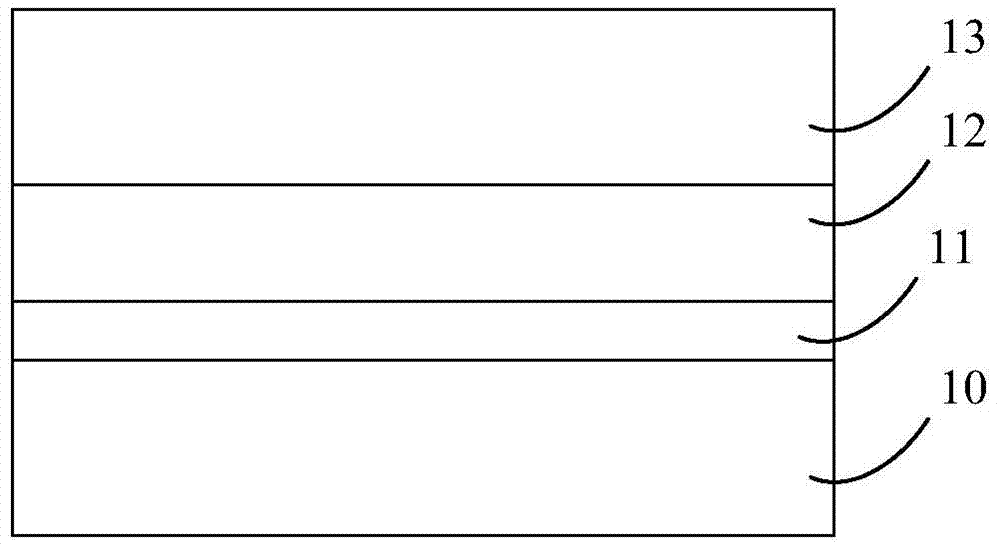
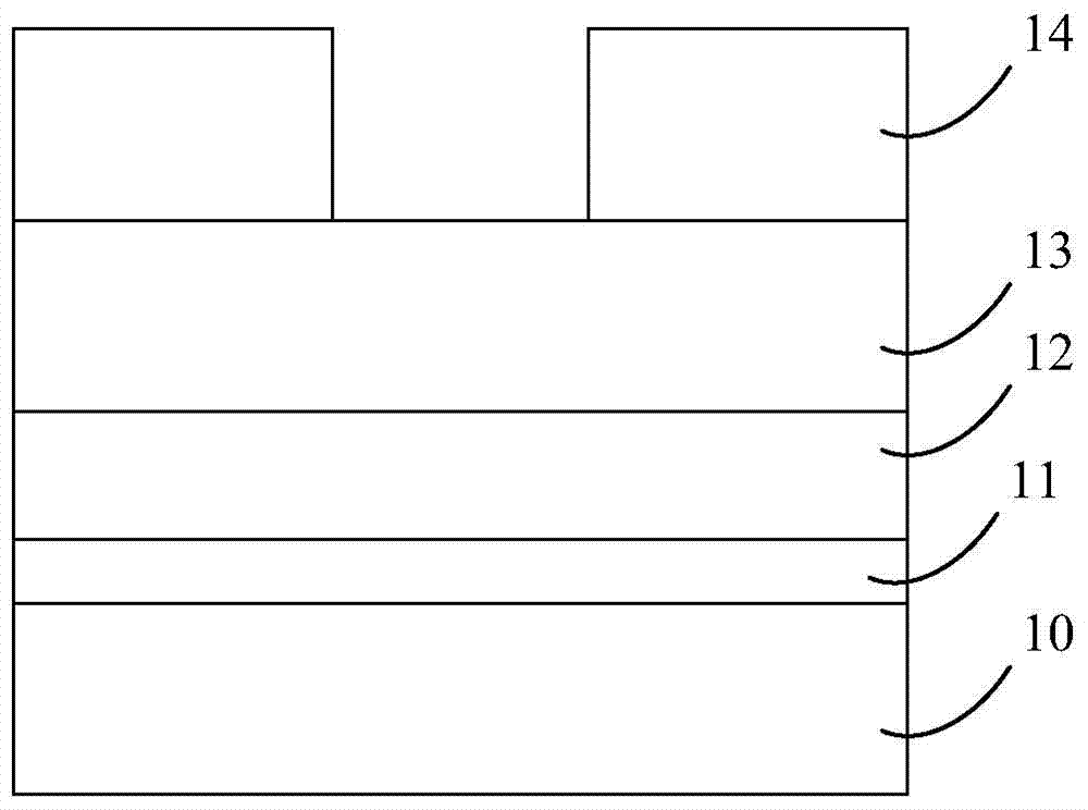
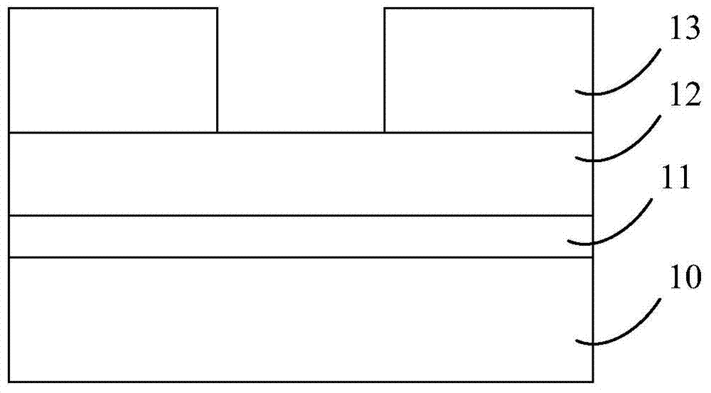
[0032] The manufacturing method of MEMS device of the present invention will be described in more detail below in conjunction with schematic diagram, wherein represents preferred embodiment of the present invention, should be appreciated that those skilled in the art can revise the present invention described here, and still realize the advantage of the present invention Effect. Therefore, the following description should be understood as the broad knowledge of those skilled in the art, but not as a limitation of the present invention.

[0033] In the interest of clarity, not all features of an actual implementation are described. In the following description, well-known functions and constructions are not described in detail since they would obscure the invention with unnecessary detail. It should be appreciated that in the development of any actual embodiment, numerous implementation details must be worked out to achieve the developer's specific goals, such as changing from...


PUM

PropertyMeasurementUnit
thicknessaaaaaaaaaa

Abstract

The invention discloses a making method of an MEMS device. The method comprises the following steps: providing a front end structure, wherein the front end structure comprises a substrate, and an AMR layer and a tantalum nitride layer which are sequentially formed on the substrate; forming a first barrier layer on the front end structure; forming a second barrier layer on the first barrier layer; etching the second barrier layer to form a first groove in order to expose the first barrier layer; and etching parts of the thickness of the exposed first barrier layer to form a second groove. The first barrier layer protects the tantalum nitride layer, avoids erosion to the tantalum nitride layer in the etching process, avoids reactions of light resistance with the tantalum nitride layer, and improves the performances of the obtained MEMS device.

Description

technical field [0001] The invention relates to the technical field of semiconductors, in particular to a manufacturing method of a MEMS device. Background technique [0002] In recent years, with the development of micro-electromechanical system (Micro-Electrico-Mechanical-System, MEMS) technology, various micro-electromechanical devices, including: micro-sensors, micro-actuators, etc., have achieved miniaturization, which is beneficial to Improve device integration, so MEMS has become one of the main development directions. [0003] Nowadays, microelectromechanical systems manufactured using anisotropic magnet resistive (AMR) have the characteristics of high sensitivity, good thermal stability, low material cost, and simple preparation process, and have been widely used. Please refer below as Figure 1-4 A schematic diagram of the structure of the MEMS device in the prior art shown. [0004] Such as figure 1 As shown, firstly, a front-end structure is provided, specifi...

Claims


Application Information

Patent Timeline
Patent Type & Authority Patents(China)
IPC IPC(8): B81C1/00
Inventor 张振兴奚裴熊磊
Owner SHANGHAI HUAHONG GRACE SEMICON MFG CORP
Why Eureka
Try Eureka