A method for laying a seed crystal, a method for preparing a quasi-single crystal silicon wafer, and a quasi-single crystal silicon wafer
A laying method, quasi-single crystal technology, applied in the direction of single crystal growth, chemical instruments and methods, crystal growth, etc. Dislocation sources and other issues, to achieve the effect of simple and easy operation of the laying method, reduction of lattice mismatch stress, and reduction of the probability of dislocations
- Summary
- Abstract
- Description
- Claims
- Application Information
AI Technical Summary
Problems solved by technology
Method used
Image
Examples
Embodiment 1
[0075] A method for laying a seed crystal, which is used for the casting of a quasi-single crystal, comprises the following steps:
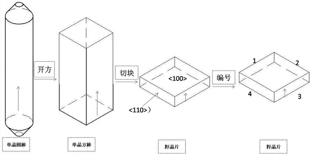
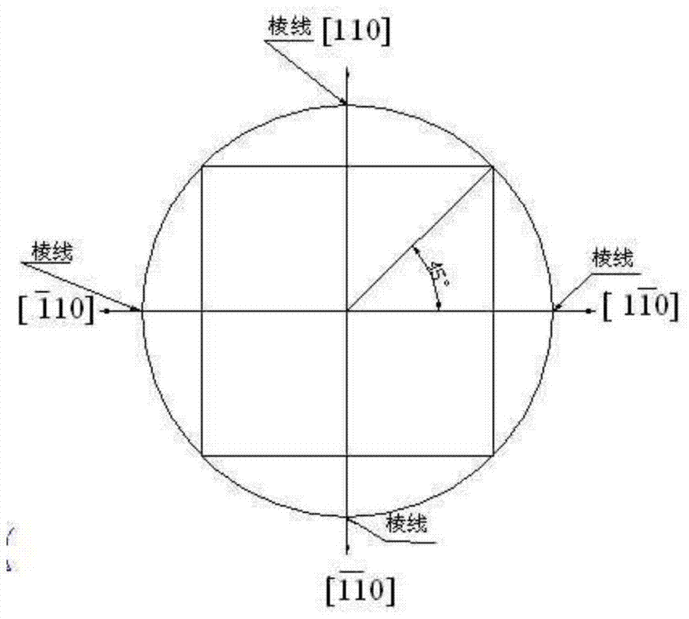
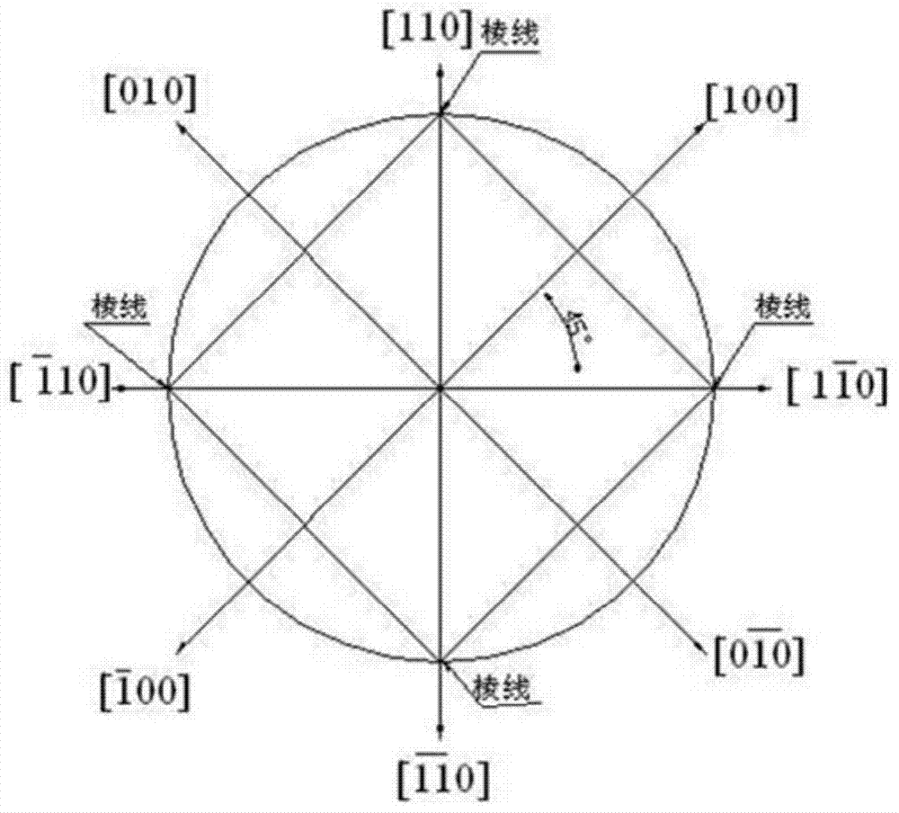
[0076] Select a square seed crystal with a crystal orientation of on the growth surface and on the side surface as the target growth seed crystal, and the numbering method is as follows figure 1 As shown, wherein, the seed crystals are derived from the same single crystal rod, the thickness of the seed crystals is 20mm, and 25 pieces of the seed crystals with a cross-sectional size of 156mm*156mm are spread on the bottom of the crucible in a 5×5 manner, and the seed crystals are The crystal growth face of the crystal is [001] with the same positive direction, and then one of the adjacent seed crystals is turned 180° around the normal direction of the contact side of the seed crystal, or one of the adjacent seed crystals is Flip 180° around the direction perpendicular to the normal direction of the contact side of the seed crystal. At this time,...
Embodiment 2
[0081] A method for laying a seed crystal, which is used for the casting of a quasi-single crystal, comprises the following steps:
[0082] Select a square seed crystal with a crystal orientation of on the growth surface and on the side surface as the target growth seed crystal, and the numbering method is as follows figure 1As shown, wherein, the seed crystals are derived from the same single crystal rod, the thickness of the seed crystals is 20mm, and 25 pieces of the seed crystals with a cross-sectional size of 156mm*156mm are spread on the bottom of the crucible in a 5×5 manner, and the seed crystals are The crystal orientation of the growth surface of the crystal is the same as [001], and then one of the adjacent seed crystals is rotated by 90°. At this time, the crystal orientation of the contact side of the two adjacent seed crystals belongs to the other crystal orientation group of the same crystal orientation group. crystal orientation, and the contact side surfaces...
Embodiment 3
[0088] A method for laying a seed crystal, which is used for the casting of a quasi-single crystal, comprises the following steps:
[0089] Select the crystallographic orientation of the growth plane as The square seed crystal with side crystal direction is used as the target growth seed crystal, and the numbering method is as follows figure 1 As shown, wherein, the seed crystals are derived from the same single crystal rod, the thickness of the seed crystals is 20mm, and 25 pieces of the seed crystals with a cross-sectional size of 156mm*156mm are spread on the bottom of the crucible in a 5×5 manner, and the seed crystals are The growth planes of the crystals are all opposite Then rotate one of the adjacent seed crystals by 90° (at this time, the adjacent seed crystals are laid on the opposite side), and at this time, the crystal orientations of the contact sides of the two adjacent seed crystals belong to different crystal orientations of the same crystal plane family i...
PUM
| Property | Measurement | Unit |
|---|---|---|
| thickness | aaaaa | aaaaa |
| thickness | aaaaa | aaaaa |
Abstract
Description
Claims
Application Information


