Magnetron sputtering chamber and magnetron sputtering equipment

A magnetron sputtering and chamber technology, used in sputtering plating, ion implantation plating, coating and other directions, can solve the problems of inability to meet the requirements of film thickness uniformity, small quantity, uneven film thickness, etc. Increased control flexibility, increased film thickness, improved uniformity

Active Publication Date: 2017-12-19
BEIJING NAURA MICROELECTRONICS EQUIP CO LTD
View PDF4 Cites 0 Cited by
  • Summary
  • Abstract
  • Description
  • Claims
  • Application Information

AI Technical Summary

Problems solved by technology

[0004] For the standard PVD (Physical Vapor Deposition) chamber, this kind of chamber is a short-range chamber with a target-base distance between 30 and 80mm, and because of the need to obtain a low-stress film, a higher chamber pressure is often used, and a higher chamber pressure is used. High chamber pressure results in fewer particles being deposited on the edge regions of the substrate than in the center, resulting in non-uniform film thickness
In this case, the effect of only relying on the magnetron 12 to improve the uniformity of the film thickness is limited, so that it cannot meet the requirements for the high uniformity of the film thickness.

Method used


Image

  • Magnetron sputtering chamber and magnetron sputtering equipment
  • Magnetron sputtering chamber and magnetron sputtering equipment
  • Magnetron sputtering chamber and magnetron sputtering equipment

Examples


Embodiment Construction

[0037] In order for those skilled in the art to better understand the technical solution of the present invention, the magnetron sputtering chamber and the magnetron sputtering equipment provided by the present invention will be described in detail below with reference to the accompanying drawings.

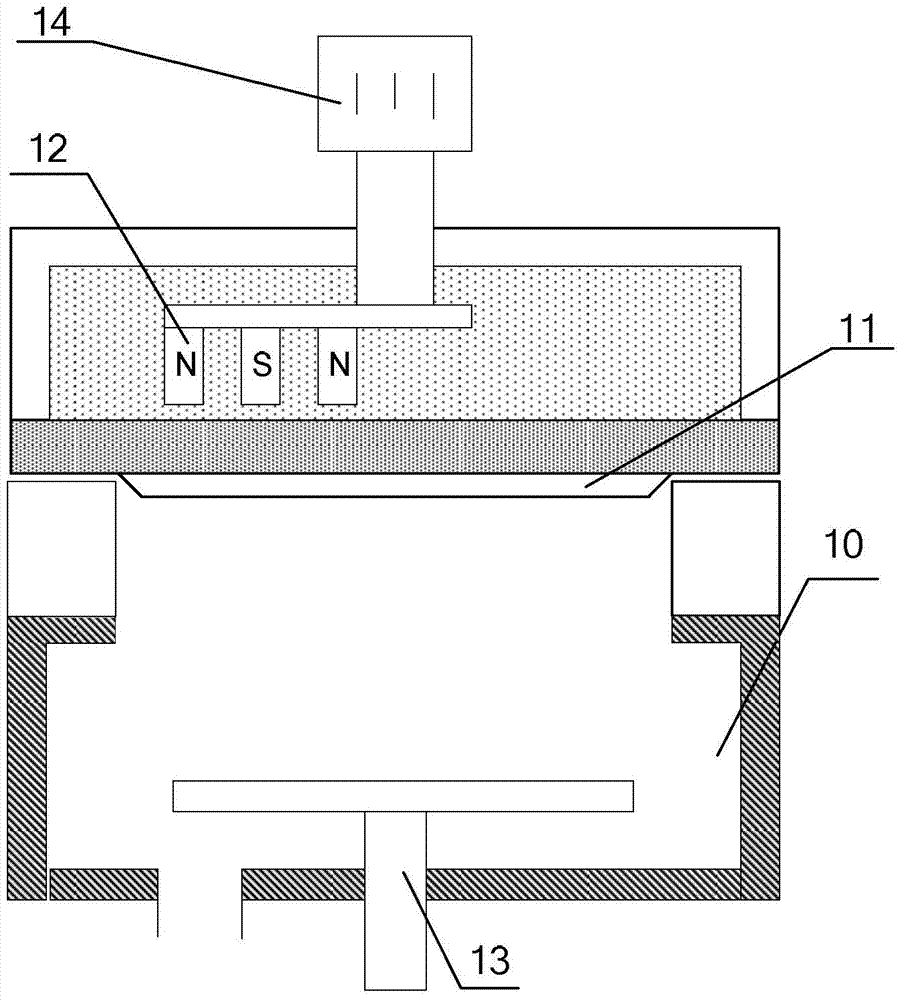
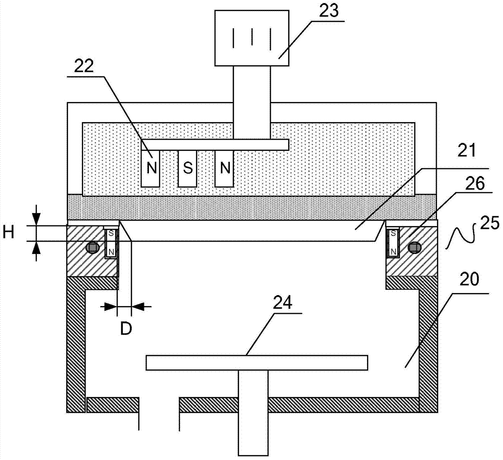
[0038] figure 2It is a sectional view of the magnetron sputtering chamber provided by the first embodiment of the present invention. see figure 2 , the magnetron sputtering chamber 20 includes a target 21 arranged on its top, a magnetron 22 arranged above the target 21, a base 24 arranged inside and below the target 21, a carrier 26 and an annular magnet assembly 25 . Among them, the target 21 is electrically connected to the sputtering power supply (not shown in the figure); the base 13 is used to carry the substrate; the magnetron 22 is connected to the magnetron driving mechanism 23, and during the sputtering deposition process , the sputtering power supply outputs sputter...


PUM


Abstract

The magnetron sputtering chamber and magnetron sputtering equipment provided by the present invention include a carrier and a ring magnet assembly, wherein the carrier is used to carry the ring magnet assembly and make it compatible with the plasma in the magnetron sputtering chamber Isolation; the ring magnet assembly surrounds the periphery of the target and is located close to the target to generate an auxiliary magnetic field that can increase the magnetic field strength in the edge area of ​​the target during the sputtering deposition process, thereby increasing self-target The number of particles sputtered from the edge area of ​​the target material can be reduced, and the number of particles sputtered from the center area of ​​the target can be reduced, thereby increasing the film thickness of the edge area of ​​the substrate and reducing the film thickness of the center area of ​​the substrate. The magnetron sputtering chamber provided by the present invention can not only adjust the distribution and intensity of the magnetic field generated in the magnetron sputtering chamber more flexibly, but also can increase the thickness of the film under the premise of obtaining a low-stress film. Uniformity.

Description

technical field [0001] The invention relates to the technical field of semiconductor processing, in particular to a magnetron sputtering chamber and magnetron sputtering equipment. Background technique [0002] In the semiconductor industry, magnetron sputtering deposition technology, as one of the important means of manufacturing thin films, is widely used in copper interconnection technology, through-silicon via technology in the packaging field, and other process fields. In practical applications, it is usually necessary to use a higher chamber pressure for the sputtering deposition process to obtain a low-stress film, so as to avoid adverse effects on the substrate due to excessive film stress. However, higher chamber pressures lead to a reduced free path for particles sputtered from the target, resulting in fewer particles being deposited on the edge regions of the substrate, resulting in less uniform film thickness. [0003] figure 1 It is a structural schematic diag...

Claims


Application Information

Patent Timeline
Patent Type & Authority Patents(China)
IPC IPC(8): C23C14/35
CPCC23C14/35H01J37/3405H01J37/3455H01J37/3461
Inventor 杨玉杰邱国庆王厚工
Owner BEIJING NAURA MICROELECTRONICS EQUIP CO LTD
Why Eureka
Try Eureka