Sputtering device

A sputtering device and sputtering gas technology, applied in the field of sputtering devices, can solve the problems of low sputtering rate, target material damage, ion damage affecting the substrate, etc. The effect of body density

Inactive Publication Date: 2015-09-30
SCREEN HLDG CO LTD
View PDF6 Cites 3 Cited by
  • Summary
  • Abstract
  • Description
  • Claims
  • Application Information

AI Technical Summary

Problems solved by technology

The sputtering rate is improved by increasing the target voltage, but there is a problem that the target material is damaged due to heat generation due to an increase in the current density of the cathode, or the ion damage caused by the target voltage spreads to the substrate ("substrate")
On the other hand, if the target voltage is suppressed in order to suppress damage to the target, there is a problem that the sputtering rate is low

Method used


Image

  • Sputtering device
  • Sputtering device
  • Sputtering device

Examples


no. 1 approach >

[0069]

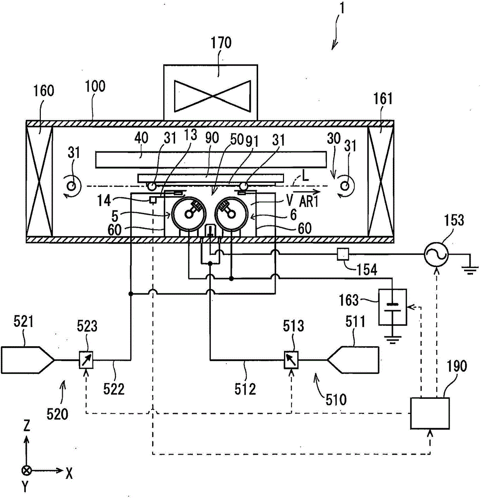
[0070] figure 1 It is a cross-sectional schematic diagram schematically showing the schematic structure of the sputtering apparatus 1 of 1st Embodiment. The sputtering apparatus 1 is an apparatus for forming a thin film on an object with a film (here, for example, the substrate 91 ) by reactive sputtering. Base material 91 is formed of, for example, a silicon wafer or the like.

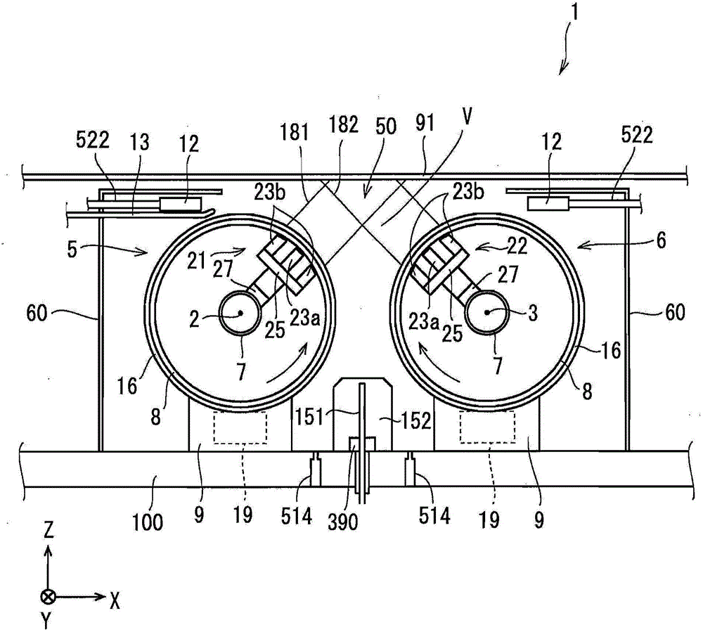
[0071] The sputtering device 1 has: a chamber (also referred to as "vacuum chamber") 100; a sputtering source 50 disposed inside the chamber 100; a transport mechanism 30 for transporting a substrate 91; a control unit 190 for The entire sputtering device 1 is uniformly controlled. The chamber 100 is a hollow member having a rectangular parallelepiped shape. The upper surface of the floor of the chamber 100 is in a horizontal posture. In addition, the X-axis and the Y-axis are respectively axes parallel to the side walls of the chamber 100 . In the description of the embodiment, the ve...

no. 2 approach >

[0126] Figure 8 It is a schematic cross-sectional view showing the periphery of the sputtering source 50A of the sputtering apparatus 1A of the second embodiment. The sputtering device 1A differs from the sputtering device 1 in that the sputtering device 1A has a rotating cathode 5A instead of the rotating cathodes 5, 6, and has a plurality of inductively coupled antennas ("high-density plasma sources") 151A instead of multiple An inductively coupled antenna 151. A plurality of inductively coupled antennas 151A are arranged at intervals along the longitudinal direction of the rotating cathode 5A. In addition, 1 A of sputtering apparatuses has each nozzle 514 corresponding to each inductive coupling antenna 151A only between the inductive coupling antenna 151A and the rotating cathode 5A.

[0127] The rotating cathode 5A has the same structure as the rotating cathode 5 except that it has a magnet unit 29 instead of the magnet unit 21 . The magnet unit 29 has the same struct...

no. 3 approach >

[0130] Figure 9 It is a cross-sectional schematic diagram showing the periphery of the sputtering source 50B of the sputtering apparatus 1B of the third embodiment. Figure 10 It is a schematic plan view showing the inductive coupling antenna 151B of the sputtering apparatus 1B.

[0131] The sputtering apparatus 1B differs from the sputtering apparatus 1 in that the sputtering apparatus 1B has a plurality (four in the illustrated example) of inductively coupled antennas 151B arranged along the longitudinal direction of the rotating cathode 5A instead of a plurality of The antenna 151 is inductively coupled, and a plurality of nozzles 12 are provided only on the upstream side of the rotating cathode 5A on the conveyance path L. In addition, in the sputtering apparatus 1B, a pair of nozzles 514 are provided on the upstream side and the downstream side of each inductively coupled antenna 151B on the conveyance path L, and the pair of nozzles 514 are arranged in the direction (Y...


PUM

PropertyMeasurementUnit
Inductanceaaaaaaaaaa

Abstract

The invention provides a sputtering device which restrains target injuries and improves sputtering rate. The sputtering device is provided with a vacuum chamber which is provided with a processing space inside, a sputtering gas supply portion which provides sputtering gas to the processing space, a first mechanism used to make the base material of a film forming object opposite to the processing space, a cylindrical rotating cathode which is arranged in the processing space and can rotate with a central axis as a center, the periphery of the rotating cathode being covered by a target material, a magnetic field forming portion which is arranged in the rotating cathode and forms a magnetic field near the part of the outer peripheral surface of the rotating cathode, the part being opposite to the base material, a rotation drive portion which makes the rotating cathode rotate relative to the magnetic field forming portion with the central axis as a center, a power supply used for sputtering, the power supply applying sputtering voltage on the rotating cathode, a high-density plasma source which generates high-density plasma in the space of the processing space, the space including the part with the magnetic field, and a high-frequency power supply which supplies high frequency electricity for the high-density plasma source.

Description

technical field [0001] The present invention relates to a sputtering device for forming a film by sputtering. Background technique [0002] A sputtering device having a magnetron rotating cathode covered with a target material on its outer peripheral surface has a high film forming rate and has an exceptionally high target use efficiency compared with a conventional flat-plate magnetron sputtering device, thereby attracting attention. attention. [0003] Patent Document 1 discloses a sputtering apparatus that has a magnetron rotating cathode in a processing space, reacts a reaction gas introduced into the processing space with a target material sputtered from the rotating cathode, and forms a film on a substrate. . [0004] Patent Document 2 discloses a sputtering apparatus having a magnetron rotating cathode in a first processing space (film formation process area) and having an inductively coupled plasma generated from outside the second processing space (reaction proces...

Claims


Application Information

Patent Timeline
IPC IPC(8): C23C14/34
CPCC23C14/354
Inventor 中岛直人羽田浩二吉野裕文
Owner SCREEN HLDG CO LTD
Why Eureka
Try Eureka