Built-in nanochannel cooling quantum cascade semiconductor laser and its preparation method

A quantum cascade, nanochannel technology, applied in semiconductor lasers, lasers, phonon exciters, etc., can solve the problem of heat dissipation of terahertz quantum cascade lasers, and achieve direct heat dissipation, single optical mode, and high cooling efficiency. Effect

Active Publication Date: 2018-03-13
吉光半导体科技有限公司
View PDF6 Cites 0 Cited by
  • Summary
  • Abstract
  • Description
  • Claims
  • Application Information

AI Technical Summary

Problems solved by technology

[0006] In order to solve the problems existing in the prior art, the present invention provides a built-in nano-channel cooling quantum cascade semiconductor laser and its preparation method, which mainly solves the heat dissipation problem of the terahertz quantum cascade laser on the chip scale. The fabrication method is applicable to edge-emitting lasers, surface-emitting lasers and terahertz quantum cascade lasers

Method used


Image

  • Built-in nanochannel cooling quantum cascade semiconductor laser and its preparation method
  • Built-in nanochannel cooling quantum cascade semiconductor laser and its preparation method
  • Built-in nanochannel cooling quantum cascade semiconductor laser and its preparation method

Examples


Embodiment 1

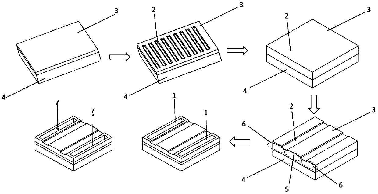
[0034] like image 3 As shown, the preparation method of the built-in nanochannel cooling terahertz quantum cascade semiconductor laser includes the following steps:

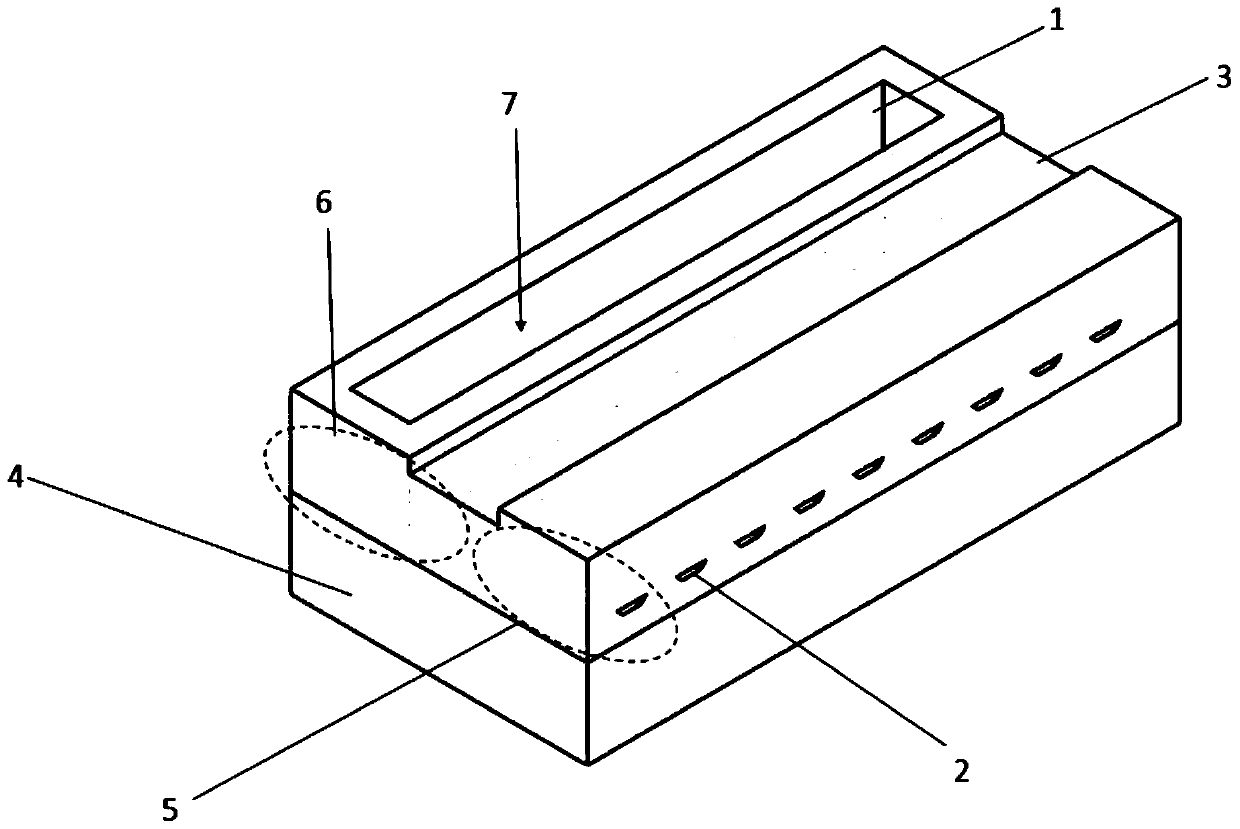
[0035] Step 1: On the part of the terahertz quantum cascade laser core layer 2 that has been grown and manufactured, by photolithography or electron beam exposure, prepare the exposure and etching according to the distribution of the designed built-in nanochannels 2, one-time A trench with a width of 300nm, a depth of 300nm, a sidewall inclination angle of 60°, and a trench length of 1200 μm was etched.

[0036] Step 2: The built-in nanochannel 3 is grown to form the built-in nanochannel 3 by using the growth rate of different crystal orientations by the method of secondary epitaxial growth, and the epitaxy is continued until the top surface is leveled, and then the core layer 3 of the terahertz quantum cascade laser is continued to be prepared.

[0037] Step 3: In the spanning length of 1.6mm, including photol...

Embodiment 2 and Embodiment 3

[0040] The preparation method of the built-in nano-channel cooling terahertz quantum cascade semiconductor laser comprises the following steps:

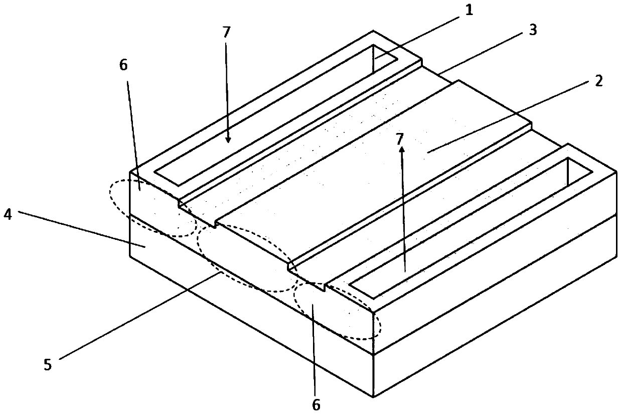
[0041] Step 1: On the substrate 4, by means of photolithography or electron beam exposure, prepare the distribution pattern of the designed built-in nanochannels 2 for exposure and etching, and etch the groove structure at one time.

[0042] Step 2, by secondary epitaxial growth, using the different growth rates of different crystal orientations, to grow and form the built-in nanochannel 3, and continue the epitaxy until the top surface of the substrate 4 is leveled, and then continue to prepare the terahertz quantum cascade laser core Layer 3.

[0043] Step 3, complete the usual semiconductor laser process steps such as photolithography, etching, making insulating layer, overlay, making electrode window, making P-side electrode, substrate thinning and optical sectioning, preparing N-side electrode, etc., to prepare terahertz quantum...


PUM


Abstract

The built-in nano-channel cooling quantum cascade semiconductor laser and its preparation method belong to the technical field of new quantum cascade lasers, and the laser includes: diversion holes, built-in nano-channels, terahertz quantum cascade laser core layers and substrates; The core layer of the terahertz quantum cascade laser includes the optical waveguide and the non-luminous chip area; the core layer of the terahertz quantum cascade laser is fabricated on the substrate; the guide hole is made on the non-luminous chip area, and its depth runs through the terahertz quantum cascade Multiple built-in nano-channels in the laser are smaller than the sum of the core layer and substrate thickness of the terahertz quantum cascade laser. The invention directly cools the chip, has high cooling efficiency, and avoids heat dissipation difficulties caused by the thermal resistance of the substrate. The built-in nanochannel can be fabricated on the substrate or inside the core layer of the semiconductor laser. By selecting a suitable working substance, the operation of THz quantum cascade lasers at different temperatures can be realized.

Description

technical field [0001] The invention belongs to the technical field of novel terahertz quantum cascade lasers, and in particular relates to a built-in nano-channel cooling terahertz quantum cascade semiconductor laser and a preparation method thereof. Background technique [0002] Terahertz quantum cascade lasers are currently being more and more widely used in national defense, information security, detection, medical treatment, communication, national defense and other fields. However, due to their small size, high power, high heat generation, and difficult heat dissipation, they have been It affects the service life and device stability of terahertz quantum cascade lasers, so room temperature lasing has not been realized so far. [0003] In terahertz quantum cascade lasers, the main heat generation mechanisms include heat generation by resistance, heat generation by photon absorption, and heat generation by energy exchange between energy levels and lattices. Heat is main...

Claims


Application Information

Patent Timeline
Patent Type & Authority Patents(China)
IPC IPC(8): H01S5/34H01S5/024
Inventor 陈泳屹秦莉宁永强王立军佟存柱单肖楠
Owner 吉光半导体科技有限公司
Why Eureka
Try Eureka