Flip LED packaging structure and manufacturing method

A technology of LED packaging and manufacturing methods, which is applied in the direction of semiconductor devices, electrical components, circuits, etc., can solve the problems of restricting the development of LED miniaturization, restricting the application of LEDs, and the large volume of packaged finished products, achieving small package size, high production efficiency, The effect of low packaging cost

Active Publication Date: 2015-10-14
HUATIAN TECH KUNSHAN ELECTRONICS
View PDF7 Cites 9 Cited by
  • Summary
  • Abstract
  • Description
  • Claims
  • Application Information

AI Technical Summary

Problems solved by technology

[0003] The current packaging form of LED flip chips is usually carried out in a single form, that is, the cut LED flip chips are mounted on the substrate (such as metal brackets, lead frames, ceramic substrates, metal substrates) one by one, and then metalized one by one. Lead interconnection, glue dispensing one by one; ...

Method used


Image

  • Flip LED packaging structure and manufacturing method
  • Flip LED packaging structure and manufacturing method
  • Flip LED packaging structure and manufacturing method

Examples


Embodiment 1

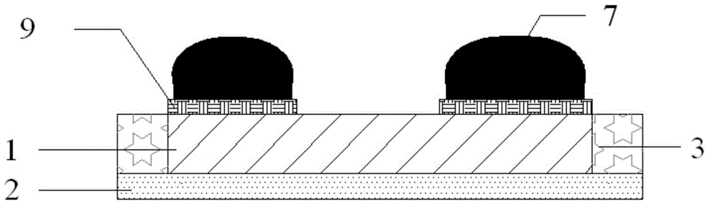
[0083] Such as figure 2 As shown, a flip-chip LED packaging structure includes an LED flip-chip 1, and the LED flip-chip has an electrode surface 101, a light-emitting surface 102 opposite to the electrode surface, and a peripheral side surface 103;

[0084] The electrode surface is not wrapped with an upper surrounding layer, and the exposed electrode 9 of the LED flip chip is provided with a solder bump 7;

[0085] The light-emitting surface is wrapped with a lower surrounding layer, and the lower surrounding layer is a single-layer structure. The single-layer structure is a layer of fluorescent layer 2. The fluorescent layer is used to convert the light emitted by the chip from fluorescent materials to white light. The fluorescent layer can be made of Phosphor powder, or transparent glue mixed with phosphor powder, or a dry film made of fluorescent material.

[0086] Optionally, the single-layer structure can also be a layer of fluorescent glass fiber composite layer 12 ....

Embodiment 2

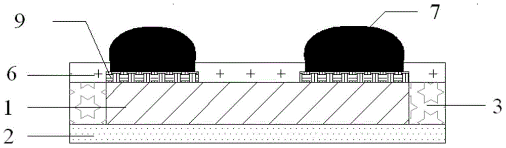
[0091] Such as image 3 As shown, this embodiment 2 includes all the technical features of embodiment 1, the difference is that the electrode surface is wrapped with an upper surrounding layer, the upper surrounding layer is a layer of protective layer 6, and the protective layer is provided with an opening , the opening exposes the electrode 9 of the LED flip chip 1 , and the solder bump 7 is arranged on the electrode. The protective layer can isolate water vapor, air, etc., and avoid corrosion of electrodes or connecting electrode metal materials. The material of the protective layer 6 includes one or more of high molecular polymers such as epoxy resin, silicon oxide, silicon nitride, and plastic packaging materials. kind.

Embodiment 3

[0093] Such as Figure 4 As shown, this embodiment 3 includes all the technical features of embodiment 2, and the difference is that the light-emitting surface is wrapped with a lower surrounding layer, and the lower surrounding layer has a two-layer structure, and the light transmission is strengthened sequentially from the inside to the outside. layer 3 and fluorescent layer 2; the surrounding side is wrapped with a surrounding layer, and the surrounding layer is a two-layer structure, which is the light transmission strengthening layer 3 and the fluorescent layer 2 in sequence from the inside to the outside. The light-transmitting strengthening layer is used to transmit light and increase the mechanical strength of the chip, and the fluorescent layer is used to convert the side light of the chip from fluorescent material to white light; that is, to realize the function of increasing the mechanical strength of the chip while changing the color of the light-emitting surface an...


PUM

PropertyMeasurementUnit
Thicknessaaaaaaaaaa

Abstract

The invention discloses a flip LED packaging structure and a manufacturing method. The electrode surface of the LED flip chip in the packaging structure is coated or not coated with an upper surrounding layer, and the electrode of the LED flip chip is connected with a solder convex block; the light-emitting surface and each side surface of the LED flip chip are embedded in a lower surrounding layer in a multilayer or two-layer or a single-layer structure and a peripheral surrounding layer; the peripheral surrounding layer is used for adjusting function applications of the chip or enhancing the mechanical strength of the chip, the lower surrounding layer is used for adjusting the color of the emitted light and enhancing the mechanical strength of the chip, and the electrode is connected with an external device via the solder convex block. Structures such as a silicon substrate or a silicon through hole are saved, technological advantages that the structure is simple, the thickness is thin, the mechanical strength is good, the packaging size is small and the like are provided, the light emitting surface and the light emitting color can be changed, the light emitting rate is improved, and function applications of the chip are multiple. According to the manufacturing method, the flip technology and the wafer level packaging technology are adopted, the silicon through hole technology is avoided during the manufacturing process, the process is simple, and the packaging cost is lower.

Description

technical field [0001] The invention relates to a packaging structure and a manufacturing method of an LED flip-chip, in particular to a packaging structure and a manufacturing method of a flip-chip LED. Background technique [0002] As a new type of high-efficiency solid-state light source, light-emitting diode (LED) has a series of advantages such as low operating voltage, low power consumption, stable and reliable performance, and has shown great potential as a lighting source. The structures of commonly used LED packaging chips in the market are: planar structure chips, that is, the positive and negative electrodes of the chip are on the light-emitting surface of the chip; vertical structure chips, that is, the positive and negative electrodes of the chip are distributed on the light-emitting surface of the chip and The two different surfaces of the reflective surface; flip chip, that is, the positive and negative electrodes of the chip are on the reflective surface of t...

Claims


Application Information

Patent Timeline
IPC IPC(8): H01L33/40
CPCH01L33/405H01L2933/0016H01L33/505H01L33/486H01L33/502H01L33/56H01L2933/0041H01L2933/005H01L2933/0066H01L33/0095H01L33/62
Inventor 万里兮肖智轶沈建树崔志勇翟玲玲钱静娴
Owner HUATIAN TECH KUNSHAN ELECTRONICS
Why Eureka
Try Eureka