Single nanometer pile face preparation method of crystalline silicon solar cell

A nano-suede and solar cell technology, which is applied in the field of solar cells, can solve the problems such as the uselessness of nano-suede, and achieve the effects of simple and easy preparation method, reduction of catalytic metal consumption, and improvement of production efficiency.

Active Publication Date: 2015-10-28
JIA XING SHANGNENG PHOTOVOLTAIC MATERIALS SCI & TECH CO LTD
View PDF4 Cites 17 Cited by
  • Summary
  • Abstract
  • Description
  • Claims
  • Application Information

AI Technical Summary

Problems solved by technology

[0011] In the existing catalytic metal-assisted wet chemical etching method, the consumption of catalytic metal accounts for a

Method used


Image

  • Single nanometer pile face preparation method of crystalline silicon solar cell
  • Single nanometer pile face preparation method of crystalline silicon solar cell
  • Single nanometer pile face preparation method of crystalline silicon solar cell

Examples


Example Embodiment

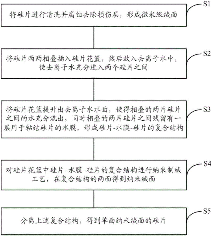
[0058] ginseng figure 1 As shown, the invention discloses a method for preparing a single-sided nano-velvet surface of a crystalline silicon solar cell, comprising the following steps:

[0059] S1. The silicon wafer is cleaned and etched to remove the damaged layer to form a micron-sized suede. The silicon chip in the present invention is a monocrystalline silicon silicon chip or a polycrystalline silicon silicon chip;

[0060] S2. Insert the silicon wafers into the wafer flower basket in two stacks, then put them into the deionized water, and move the silicon wafer flower basket up and down in the deionized water for 1 to 2 minutes, so that the deionized water can fully enter between the two silicon wafers;

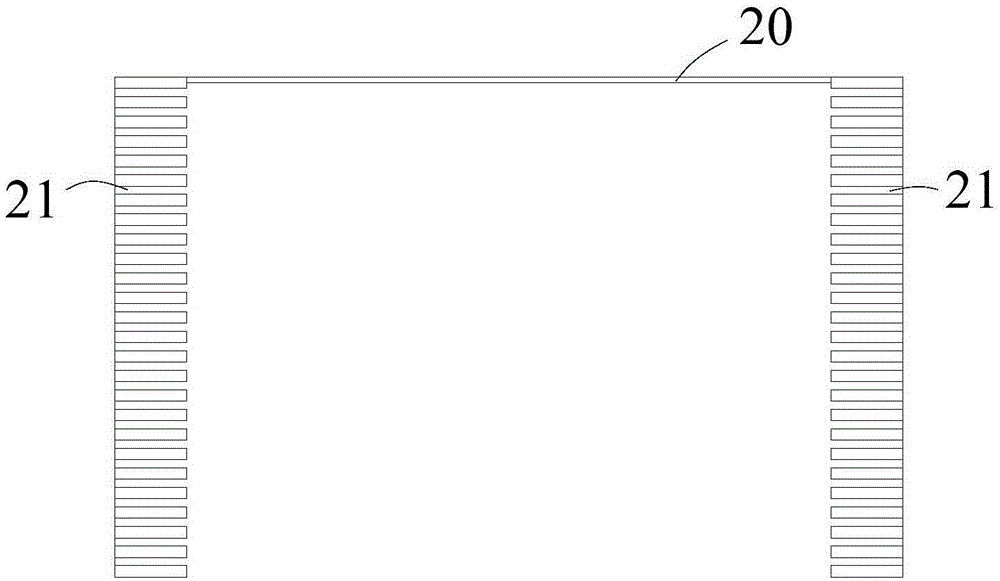
[0061] Schematic diagram of the structure of the silicon wafer flower basket 20 figure 2 As shown, it is exactly the same as the existing silicon flower basket, and the two side walls of the silicon flower basket are correspondingly provided with several slots 21. Pre...


PUM


Abstract

Disclosed in the invention is a single nanometer pile face preparation method of a crystalline silicon solar cell. The preparation method comprises the following steps: S1, cleaning and corroding silicon wafers to remove damage layers, thereby forming micron-order pile faces; S2, overlaying each two silicon wafers and then inserting the silicon wafers into a silicon wafer basket, and placing the silicon wafer basket into deionized water to enable the deionized water to enter the space the two silicon wafers completely; S3, lifting the silicon wafer basket out of the deionized water surface to enable the water between the overlaid two silicon wafers to flow out of the space and keeping a water membrane for bonding with the silicon wafers between the two overlaid silicon wafers, thereby forming a composite structure with the silicon wafer, the water membrane, and the silicon wafer successively; S4, carrying out a nanometer pile preparing process on the composite structure with the silicon wafer, the water membrane, and the silicon wafer in the silicon wafer basket to obtain nanometer pile faces at the two sides of the composite structure; and S5, separating the composite structure to obtain a silicon wafer with a single nanometer pile face. According to the invention, the half of the catalysis metal consumption can be reduced and thus the production cost is substantially lowered; the wafer installation amount is double in one basket and the production efficiency is doubled.

Description

technical field [0001] The invention relates to the technical field of solar cells, in particular to a method for preparing a single-sided nano-velvet surface of a crystalline silicon solar cell. Background technique [0002] Photovoltaic power generation is an important component of new energy, and has achieved rapid development in recent years. Among the current commercialized solar cell products, crystalline silicon (monocrystalline and polycrystalline) solar cells have the largest market share, and have maintained a market share close to 90%. [0003] At present, in the production process of crystalline silicon solar cells, the purpose of the textured process is to reduce the surface reflectance of the solar cell, thereby improving the photoelectric conversion efficiency of the solar cell. In order to obtain a textured structure with excellent performance on the surface of crystalline silicon wafers, the photovoltaic industry has tried many methods, such as mechanical g...

Claims


Application Information

Patent Timeline
IPC IPC(8): H01L31/0236
CPCY02E10/50H01L31/02363
Inventor 苏晓东叶晓亚
Owner JIA XING SHANGNENG PHOTOVOLTAIC MATERIALS SCI & TECH CO LTD
Why Eureka
Try Eureka