Perovskite-based inverted thin film solar cell and preparation method thereof
A solar cell and perovskite technology, applied in circuits, photovoltaic power generation, electrical components, etc., can solve the problems of inability to prepare flexible substrates and increase costs, and achieve the effects of low cost, good stability and low cost
- Summary
- Abstract
- Description
- Claims
- Application Information
AI Technical Summary
Problems solved by technology
Method used
Image
Examples
Embodiment 1
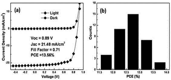
[0034] (1) the NH 2 CH=NH 2 I(FAI) and PbI 2 Mix and dissolve in N,N-dimethylformamide (DMF) solvent at a molar ratio of 1:1, stir at room temperature for 12 hours, and filter the solution with a 0.22 um organic filter head;
[0035] (2) Provide a patterned ITO conductive glass substrate. After scrubbing with detergent, use acetone, ethanol, and deionized water to ultrasonically clean each twice for ten minutes each time, and then put it in a drying oven to dry ;
[0036] (3) Ozone treatment was performed on the dried ITO conductive glass substrate, and the ozone treatment time was 15 min;
[0037](4) Spin-coat a layer of PEDOT:PSS on the surface of the ITO conductive glass substrate at a rotational speed of 4000 rpm / 40 s, and then perform annealing treatment at 140°C / 15 min (the preparation of this layer is carried out in an atmospheric environment );
[0038] (5) Transfer the ITO conductive glass substrate to the glove box and spin-coat FAPbI 3 The perovskite precursor...
Embodiment 2
[0045] (1) the NH 2 CH=NH 2 I(FAI) and PbI 2 Mix and dissolve in N,N-dimethylformamide (DMF) solvent at a molar ratio of 1:1, stir at room temperature for 12 hours, and filter the solution with a 0.22 um organic filter head;
[0046] (2) Provide a patterned ITO conductive glass substrate. After scrubbing with detergent, use acetone, ethanol, and deionized water to ultrasonically clean each twice for ten minutes each time, and then put it in a drying oven to dry ;
[0047] (3) Ozone treatment was performed on the dried ITO conductive glass substrate, and the ozone time was 15 min;
[0048] (4) Spin-coat a layer of PEDOT:PSS precursor solution on the surface of ITO at a speed of 4000 rpm / 40 s, and then perform annealing treatment at 140°C / 15 min (the preparation of this layer is carried out in an atmospheric environment) ;
[0049] (5) Transfer the ITO conductive glass substrate to the glove box and spin-coat FAPbI 3 The perovskite precursor layer was cleaned with chlorobe...
Embodiment 3
[0053] The difference between this example and Example 1 is that the hole transport layer material is graphene oxide (GO), and other steps are the same as Example 1.
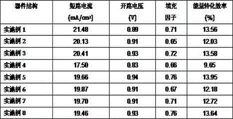
[0054] The device structure of Example 3 is ITO / GO / FAPbI3 / PCBM / BCP / Ag.
PUM
 Abstract
Description
Claims
Application Information


