Solar cell photo-anode using semiconductor thin film as sensitizing agent and preparation method of solar cell photo-anode

A technology for solar cells and semiconductors, applied in the direction of photosensitive equipment, etc., can solve the problems of less adsorption of sensitizers, poor controllability, and low coverage, and achieve improved photoelectric conversion efficiency, simple and convenient preparation methods, continuous and scalable bandgap tune effect

Inactive Publication Date: 2014-01-29
DALIAN INST OF CHEM PHYSICS CHINESE ACAD OF SCI
View PDF3 Cites 10 Cited by
  • Summary
  • Abstract
  • Description
  • Claims
  • Application Information

AI Technical Summary

Problems solved by technology

[0004] At present, semiconductor quantum dot sensitizers used in quantum dot sensitized batteries can be divided into two categories from the assembly method of solar cells. The first category is to first use chemical methods to synthesize quantum dots, and then use organic molecules to connect TiO 2 The advantage of doing this is that the quality of the obtained quantum dots is high, and the particle size is uniform and controllable. The disadvantage is that TiO 2 The adsorption amount of the upper sensitizer is small, and the sunlight cannot be effectively used; the second type is TiO 2 In situ preparation of quantum dots, the method used is chemical bath deposition (CBD) or ion alternating adsorption reaction (SILAR). The advantage is that it can increase the adsorption amount of semiconductor sensitizers, and the disadvantage is that the controllability is poor [Robel, I., et al. al., Journal of the American Chemical Society, 2006.128(7): p.2385-2393.; Lee, H., et al., Nano Letters, 2009.9(12): p.4221-4227.; Lee, H.J., et al., Chemistry of Materials, 2010.22(19): p.5636-5643.】
[0005] The study found that in the quantum dot sensitized battery, due to the semiconductor quantum dot sensitizer in TiO 2 Low coverage on the substrate, photogenerated electrons generated on the semiconductor sensitizer under light injection into TiO 2 Middle part from TiO 2 Reversely injected into the electrolyte, a recombination process occurs, which limits the further improvement of battery efficiency [Kamat, P.V., Accounts of Chemical Research, 2012.; Mora-Sero, I., et al., Accounts of Chemical Research, 2009.42(11) :p.1848-1857.]
[0006] In the literature, there has been an underpotential method used in TiO 2 CdS thin film was grown in , and its photoelectric properties were studied [Zhu, W., et al., Journal of the American Chemical Society, 2010.132(36): p.12619-12626.], but this method uses electrochemical Synthesis, complex operation, poor controllability and not easy to prepare multilayer films

Method used


Image

  • Solar cell photo-anode using semiconductor thin film as sensitizing agent and preparation method of solar cell photo-anode
  • Solar cell photo-anode using semiconductor thin film as sensitizing agent and preparation method of solar cell photo-anode
  • Solar cell photo-anode using semiconductor thin film as sensitizing agent and preparation method of solar cell photo-anode

Examples


Embodiment 1

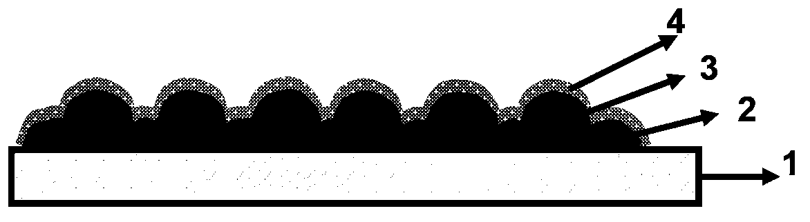
[0035] Wide bandgap semiconductor chooses TiO 2 Porous membrane composed of nanoparticles, TiO 2 The particle size is about 20nm and the thickness is about 5μm. Use dimethyl cadmium, trimethylsilthione, and trimethylsilylselenane as raw materials, high argon as carrier gas, carrier gas flow rate 100 sccm, reaction temperature 150 ° C, chamber pressure 10 -1 toor, cation and anion sources alternately enter the main chamber, and the pulse time of a single source is 0.05s. After atomic layer deposition (ALD) grows CdS / CdSe with different thicknesses, the morphology of nanotubes basically does not change, which is consistent with atomic layer deposition (ALD). Growth (conformal deposition) characteristics. using atomic layer deposition (ALD) on TiO 2 200 cycles of CdS film and 200 cycles of CdS / 200 cycles of CdSe were grown on the porous membrane, and CdS sensitized cells and CdS / CdSe co-sensitized cells were prepared respectively. The data and results are shown in the table. ...

Embodiment 2

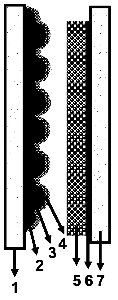
[0038] The difference from Example 1 is that the wide bandgap semiconductor uses TiO 2 A porous membrane composed of nanotube arrays, the outer diameter of nanotubes is about 110nm, the inner diameter is about 80nm, and the tube length is about 15μm. Use dimethyl cadmium, trimethylsilthione, and trimethylsilylselenane as raw materials, high argon as carrier gas, carrier gas flow rate 100 sccm, reaction temperature 150 ° C, chamber pressure 10 -1 toor, cation and anion sources alternately enter the main chamber, and the pulse time of a single source is 0.05s. After atomic layer deposition (ALD) grows CdS / CdSe with different thicknesses, the morphology of nanotubes basically does not change, which is consistent with atomic layer deposition (ALD). Growth (conformal deposition) characteristics.

[0039] Figure 5 a: Scanning electron microscope (SEM) image of the top of the nanotube before atomic layer deposition (ALD) growth of CdS / CdSe

[0040] Figure 5 b: Scanning electron...

Embodiment 3

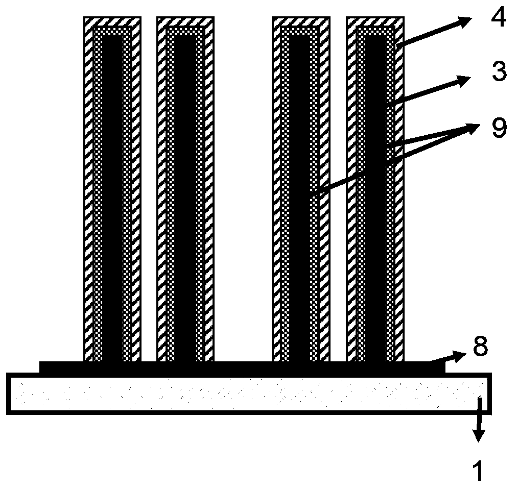
[0044] The difference from Example 1 is that the wide bandgap semiconductor uses TiO 2 A porous membrane composed of nanotube arrays, the outer diameter of nanotubes is about 110nm, the inner diameter is about 80nm, and the tube length is about 15μm. Use dimethyl cadmium and trimethylsilthione as raw materials, high argon as carrier gas, carrier gas flow rate 100 sccm, reaction temperature 150 ° C, chamber pressure 10 -1 toor, cation and anion sources alternately enter the main chamber, and the pulse time of a single source is 0.05s. After atomic layer deposition (ALD) grows CdS with different thicknesses, the morphology of nanotubes basically does not change, which is consistent with atomic layer deposition (ALD) conformal growth ( conformal deposition) features. using atomic layer deposition (ALD) on TiO 2 The sensitized battery is assembled by depositing different cycles of CdS films on the nanotubes. The short-circuit current increases with the increase of the amount of ...


PUM

PropertyMeasurementUnit
particle diameteraaaaaaaaaa
thicknessaaaaaaaaaa
thicknessaaaaaaaaaa

Abstract

The invention relates to a solar cell photo-anode using a semiconductor thin film as a sensitizing agent and a preparation method of the solar cell photo-anode. The solar cell photo-anode is composed of a photo-anode body formed by a nano metal oxide semiconductor material and semiconductor sensitizing agent thin films covered on the surface, an electrolyte capable of generating oxidation and reduction reaction and a counter electrode, the photo-anode and the counter electrode are isolated by using a heat sealable film, the electrolyte is filled between the photo-anode and the counter electrode, the electrolyte at an interface where the photo-anode contacts with the electrolyte generates oxidation reaction, and the electrolyte at an interface where the counter electrode contacts with the electrolyte generates reduction reaction. The solar cell photo-anode has the advantages that an n-type wide-band-gap semiconductor material is adopted for the photo-anode, and the photo-anode of a solar cell is formed by growing various n-type semiconductor sensitizing agent thin films on the surface of the wide-band-gap semiconductor material by using atomic layer deposition technology , so that light absorbing range of the photo-anode is greatly widened; a semiconductor thin film sensitizing layer enables a wide-band-gap semiconductor and the electrolyte to be isolated, so that compositing of photo-generated carriers at the interface is substantially reduced, and efficiency of the solar cell is remarkably improved.

Description

technical field [0001] The invention relates to a solar cell device using a semiconductor thin film as a sensitization layer. Specifically, a solar cell photoanode using a semiconductor as a sensitizer is a semiconductor sensitizer assembled by uniformly depositing multiple layers of dense narrow-bandgap semiconductor thin films on a wide-bandgap semiconductor by atomic layer deposition (ALD) as a light-absorbing layer. chemical solar cells. Background technique [0002] According to the development process, solar cells are divided into three generations. The first generation is crystalline silicon solar cells, accounting for about 80% of the current market share; the second generation is thin film batteries, such as copper indium selenium thin film batteries, cadmium telluride thin film batteries, etc. 20% market share; the concept of the third generation of solar cells has been proposed, high conversion efficiency, low cost, environmental friendliness and pollution-free a...

Claims


Application Information

Patent Timeline
Patent Type & Authority Applications(China)
IPC IPC(8): H01G9/20H01G9/042
Inventor 李灿张文华郑霄家于东麒熊锋强
Owner DALIAN INST OF CHEM PHYSICS CHINESE ACAD OF SCI
Why Eureka
Try Eureka