Scintillator photonic crystal structure and manufacturing method therefor

A technology of photonic crystals and manufacturing methods, which is applied in the field of scintillators, can solve the problems of low light output efficiency, achieve the effect of improving light transmission efficiency and reducing total reflection

Inactive Publication Date: 2015-11-18
NORTHWEST INST OF NUCLEAR TECH +1
View PDF6 Cites 18 Cited by
  • Summary
  • Abstract
  • Description
  • Claims
  • Application Information

AI Technical Summary

Problems solved by technology

[0007] In order to overcome the deficiency of low light output efficiency of existing scintillators, the present invention provides a scintillator photonic crystal structure

Method used


Image

  • Scintillator photonic crystal structure and manufacturing method therefor
  • Scintillator photonic crystal structure and manufacturing method therefor
  • Scintillator photonic crystal structure and manufacturing method therefor

Examples


Embodiment 1

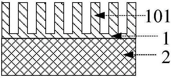
[0032]Example 1. The scintillator photonic crystal structure of the present invention includes a scintillator 2 and a photonic crystal 1. The photonic crystal 1 is closely attached to the surface of the scintillator 2. The photonic crystal 1 is composed of photonic crystal microstructures 101 arranged periodically in a hexagonal or quadrangular shape. A single photon The crystal microstructure 101 is columnar, conical, cuboid or polyhedral in shape; the distance between the photonic crystal microstructure 101 is 200-2000nm, and the height is 50-800nm. The maximum side length of the photonic crystal microstructure 101 is 100-1000nm, the width and length of the cuboid photonic crystal microstructure 101 are 100-1000nm, and the side length of the polyhedral photonic crystal microstructure 101 is 100-1000nm; the photonic crystal 1 is made of transparent The organic polymer material is cured by means of ultraviolet light, heating or irradiation; the optimal size of the photonic cry...

Embodiment 2

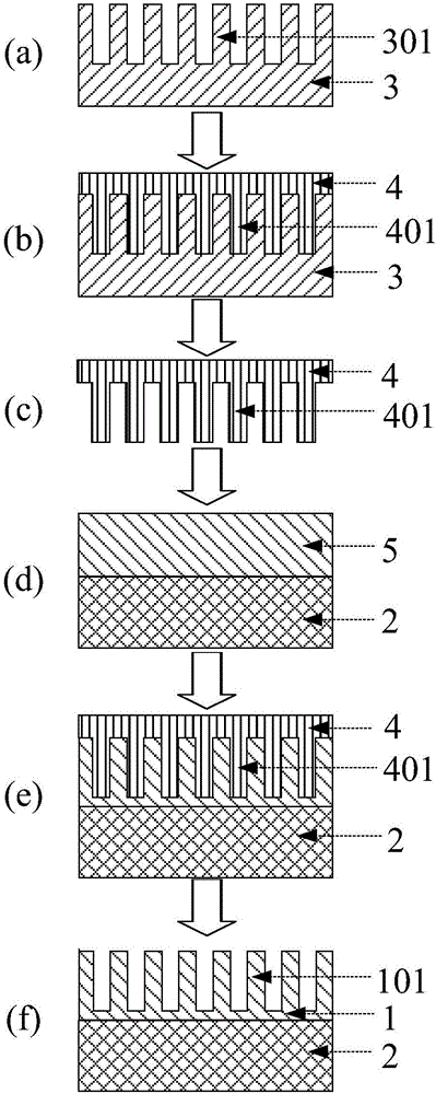
[0033] Example 2. The specific steps are carried out step by step according to the sequence indicated by the arrows (a) to (f). In the first step, the final size of the photonic crystal microstructure 101 is designed according to the material properties and luminous properties of the scintillator 2, and a forward microstructure 301 with the same size and the same arrangement as the photonic crystal microstructure 101 is fabricated on the substrate to form The positive template 3 of photon; In the second step, a layer of polydimethylsiloxane (PDMS) is coated on the positive microstructure 301 side of the positive template 3, and the polydimethylsiloxane naturally expands and fills the positive template. In the gap between the microstructures 301, the thickness of the polydimethylsiloxane is greater than the height of the forward microstructures 301; in the third step, the negative template 4 is formed after the natural curing of the polydimethylsiloxane, and the positive micros...

Embodiment 3

[0036] Example 3. The scintillator 2 is a plastic scintillation material EJ212 with a diameter of 3 cm and a thickness of 1 mm produced by the American ELJEN company; the photonic crystal 1 is composed of cylindrical photonic crystal microstructures 101 arranged in a hexagonal pattern, and the distance between adjacent cylindrical photonic crystal microstructures 101 is 600 nm. A single photonic crystal microstructure 101 has a diameter of 300nm and a height of 310nm; the substrate material of the positive template 3 is semiconductor silicon, and the forward microstructure 301 on it is made by electron beam etching process. The negative template 4 is formed by natural curing of polydimethylsiloxane coated on the surface of the positive template 3; the organic polymer 5 spin-coated on the surface of the scintillator 2 is PMMA photoresist produced by British EMResist Ltd; the negative template 4 The side with the trans-type microstructure 401 is pressed on the organic polymer 5 ...


PUM

PropertyMeasurementUnit
heightaaaaaaaaaa
diameteraaaaaaaaaa
lengthaaaaaaaaaa

Abstract

The invention discloses a scintillator photonic crystal structure and a manufacturing method therefor, and is used for solving a technical problem that a conventional scintillator is low in efficiency of light output. The technical scheme is that the scintillator photonic crystal structure comprises a scintillator and a photonic crystal; the photonic crystal consists of a series of hexagonal or quadrangular periodically-arranged photonic crystal microstructures. The method comprises the steps: positive template manufacturing, negative template manufacturing, polymer coating and solidifying, and demolding. The surface of the scintillator is provided with a periodically-arranged photonic crystal microstructure layer, wherein the size of the periodically-arranged photonic crystal microstructure layer is equivalent to the wavelength of light of the scintillator. The photonic crystal composed of the photonic crystal microstructures achieves the modulation of fluorescent light of the scintillator, thereby reducing the total reflection of the fluorescent light of the scintillator at an interface and the multiple scattering of internal light of the scintillator, enabling the fluorescent light of the scintillator to be transmitted outside from the surface of the scintillator, and improving the light output efficiency of the scintillator.

Description

technical field [0001] The invention relates to a scintillator, in particular to a scintillator photonic crystal structure. The present invention also relates to a method for manufacturing the scintillator photonic crystal structure. Background technique [0002] In the field of radiation detection, scintillators refer to substances that can produce fluorescence after interacting with radiation such as rays or particles. In layman's terms, the function of the scintillator is to convert the energy deposited in the scintillator into fluorescent photons and release them. A scintillation detector is generally composed of a scintillator and a photodetector, wherein the scintillator converts the energy deposited by radiation into fluorescent photons, and the photodetector detects the fluorescence of the scintillator and converts it into an electrical signal output, thereby realizing the detection of radiation. Information such as the type, time, energy, position, and momentum of...

Claims


Application Information

Patent Timeline
Patent Type & Authority Applications(China)
IPC IPC(8): G01T1/20
Inventor 刘金良刘波朱智超陈亮欧阳晓平程传伟胡静
Owner NORTHWEST INST OF NUCLEAR TECH
Why Eureka
Try Eureka