High pixel image sensor packaging structure and manufacturing method thereof

A technology of image sensor and packaging structure, which is applied in the direction of electric solid-state devices, semiconductor devices, radiation control devices, etc. It can solve the problems of product failure, large difference in thermal expansion coefficient, small strength and rigidity of supporting walls, etc., and achieve the reduction of impurities and particles , meet the distance requirements, and improve the effect of product yield

Inactive Publication Date: 2018-02-16
BEIJING UNIV OF TECH
View PDF4 Cites 0 Cited by
  • Summary
  • Abstract
  • Description
  • Claims
  • Application Information

AI Technical Summary

Problems solved by technology

However, due to the low strength and rigidity of the supporting wall currently used, and the poor uniformity, it is not enough to support the large distance between the glass and the image sensing area in the high-pixel sensor, which will cause poor flatness of the connection and the glass surface inequality problem
Moreover, since the glass surface is always exposed to the outside during the process, it is unavoidable that it will be contaminated with impurity particles in the air and debris generated during the process, which will deteriorate the photosensitive performance of the high-pixel image sensor and reduce the yield rate.
In addition, due to the large difference in thermal expansion coefficient between the supporting wall material and other materials, it is easy to cause delamination and cracks caused by thermal stress on the upper and lower surfaces of the supporting wall in contact with other materials, resulting in product failure

Method used


Image

  • High pixel image sensor packaging structure and manufacturing method thereof
  • High pixel image sensor packaging structure and manufacturing method thereof
  • High pixel image sensor packaging structure and manufacturing method thereof

Examples


Embodiment Construction

[0064] Specific embodiments of the present invention will be described below with reference to the accompanying drawings, wherein the corresponding structures in different embodiments use the same reference numerals, but it does not mean that there is necessarily a correlation between different embodiments and / or structures. For the convenience of illustration, some existing conventional structures are shown in simplified structures in the drawings, and the structures in the drawings are not scaled to the same scale, so they do not represent the actual relative sizes of the structures in the embodiments.

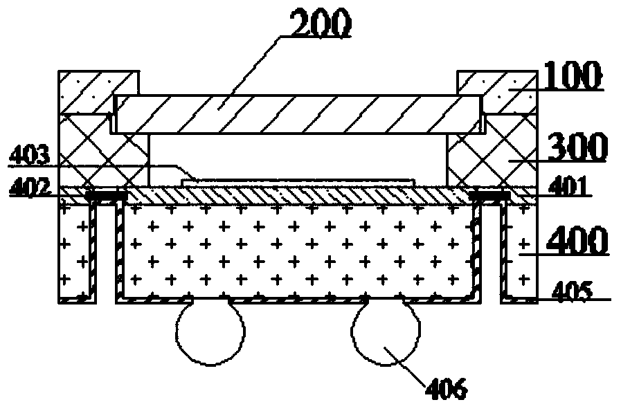
[0065] refer to figure 1 , which is a schematic diagram of a high pixel image sensor package according to an embodiment of the present invention. The structure includes:

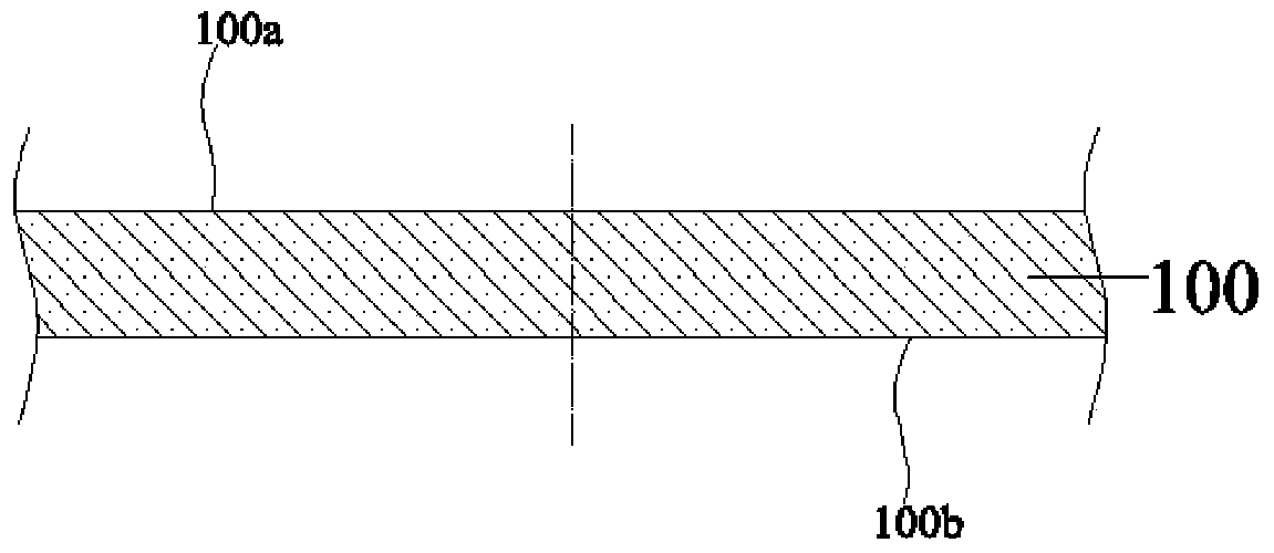
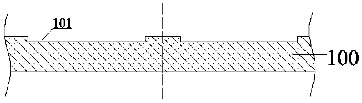
[0066] The cover plate (100) comprises a cover plate first surface (100a) and a cover plate second surface (100b), (100a), (100b) are the upper and lower surfaces of the cover plate (100); the cover plate...


PUM


Abstract

The invention provides a high-pixel image sensor packaging structure and a manufacturing method thereof. The packaging structure comprises a cover plate and a support cover plate respectively provided with a step-shaped containing structure, a transparent cover plate, and a wafer with a re-routed wire, According to the packing structure and the manufacturing method thereof, silicon or the silicon-based material with high rigidity and relatively high strength is employed as the support cover plate to replace an original support cofferdam layer made of the high-molecular material, problems of poor homogeneity and poor bonding force with contact materials after the formation of the support cofferdam layer of the high-molecular polymer are solved, the thermal stress generated due to the difference of the thermal expansion coefficient can be reduced, and failures such as layering and cracks of the structure are improved; besides, the height of the support cover plate can be set according to the practical requirement and is not limited to dozens of micrometers, and the requirement of the distance between a light transmittance cover plate and an image sensor region for the high-pixel image sensor is satisfied.

Description

technical field [0001] The invention relates to a wafer-level packaging structure and a manufacturing method thereof, in particular to a high-pixel image sensor packaging structure and a manufacturing method thereof, and belongs to the field of semiconductor packaging. Background technique [0002] An image sensor is a semiconductor module, a device that converts an optical image into an electronic signal, which can be used for further processing or digitized and stored, or used to transfer the image to another display device for display Wait. It is widely used in digital cameras and other electro-optical devices. Image sensors are now mainly divided into charge-coupled devices (CCD) and CMOS image sensors (CIS, CMOS Image Sensor). Although the CCD image sensor is superior to the CMOS image sensor in terms of image quality and noise, the CMOS sensor can be manufactured with traditional semiconductor production technology, and the production cost is relatively low. At the ...

Claims


Application Information

Patent Timeline
Patent Type & Authority Patents(China)
IPC IPC(8): H01L27/146
CPCH01L2924/16235
Inventor 秦飞史戈别晓锐安彤武伟肖智轶
Owner BEIJING UNIV OF TECH
Why Eureka
Try Eureka