Power MOS device

A MOS device and power technology, applied in the direction of semiconductor devices, electrical components, circuits, etc., can solve the problems of growth, large specific on-resistance, and increase in chip area, etc., to reduce specific on-resistance, reduce device size, Easy to Integrate Effects

Active Publication Date: 2015-11-18
UNIV OF ELECTRONICS SCI & TECH OF CHINA
View PDF13 Cites 8 Cited by
  • Summary
  • Abstract
  • Description
  • Claims
  • Application Information

AI Technical Summary

Problems solved by technology

However, compared with power VDMOS, the length of the lightly doped drift region of power LDMOS increases with the increase of breakdown voltage, resulting in a proportional increase in chip area, making LDMOS have a large specific on-resistance

Method used


Image

  • Power MOS device
  • Power MOS device
  • Power MOS device

Examples


Embodiment 1

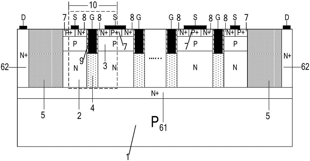
[0033] Such as figure 1 As shown, it includes a second conductivity type semiconductor substrate 1 and a first conductivity type heavily doped semiconductor drain region 61 located on the upper surface of the second conductivity type semiconductor substrate 1; the first conductivity type heavily doped semiconductor drain region 61 There are first conductivity type heavily doped semiconductor drain extension regions 62 at both ends of the upper surface; there are multiple parallel cell structures between the first conductivity type heavily doped semiconductor drain extension regions 62; the first conductivity type heavy There is a dielectric groove 5 between the doped semiconductor drain extension region 62 and the cellular structure, and the dielectric groove 5 is filled with a first dielectric layer; the cellular structure includes a gate structure, a first conductivity type semiconductor drift region 2 and The second conductivity type semiconductor body region 3; the first c...

Embodiment 2

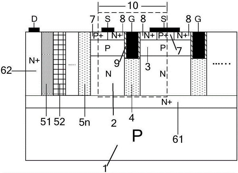
[0036] Such as figure 2As shown, the structural schematic diagram of the integrated power MOS device adopting the variable K-slot medium in this example is different from that in Embodiment 1 in that the first dielectric layer is composed of multiple media, and the dielectric constant of the media is determined by the first The heavily doped semiconductor drain extension region 62 of a conductivity type gradually increases toward the cell structure 10 side. In this embodiment, the dielectric with a high dielectric constant can enhance the auxiliary depletion of the drift region 2, optimize the distribution of equipotential lines on one side of the dielectric tank, and improve the withstand voltage of the device.

Embodiment 3

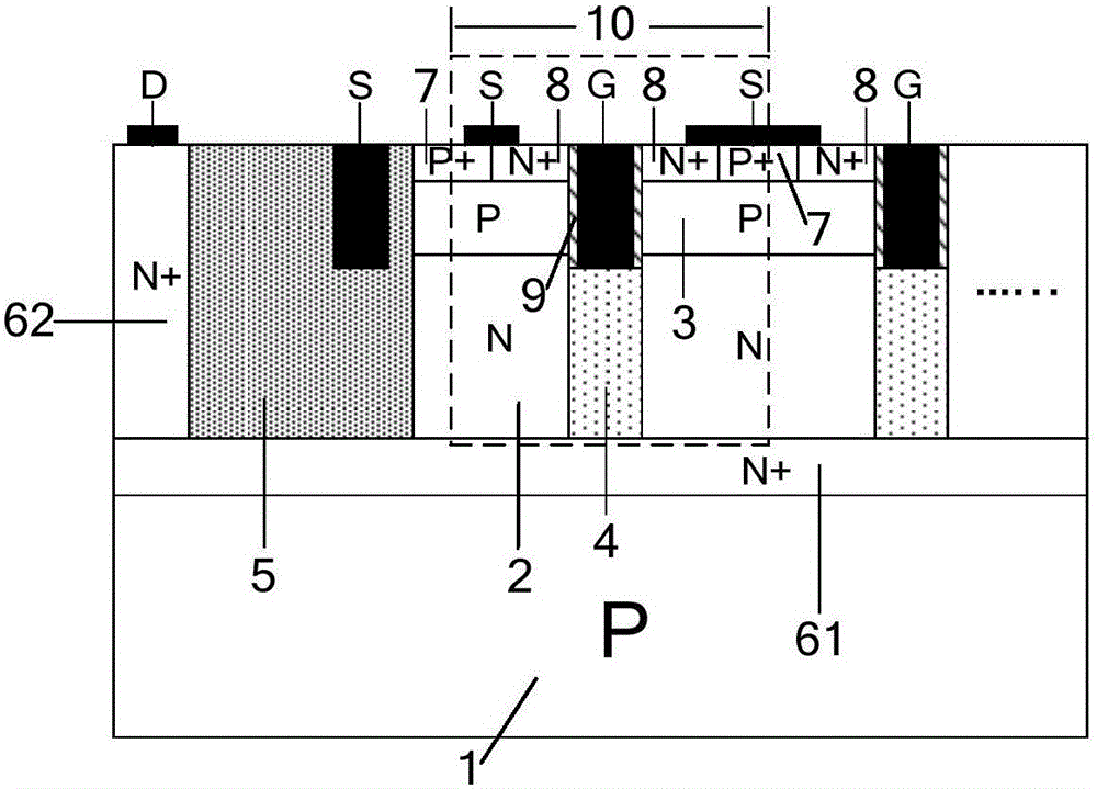
[0038] Such as image 3 As shown, the structure schematic diagram of the integrated power MOS device with the source field plate of this example is different from that of Embodiment 1 in that the dielectric trench 5 has a metallized source, and the two sides of the metallized source and The bottom is in contact with the first dielectric layer. The metallized source acts as a source field plate, which can assist in depleting the drift region 2, optimize the distribution of equipotential lines, and improve the withstand voltage of the device.


PUM


Abstract

The invention belongs to the technical field of power semiconductor devices and relates to a power MOS device. The power MOS device comprises cellular structures respectively having a high-K dielectric extension grid structure, a drain extension region, and a dielectric slot terminal. The multiple cellular structures are arranged in parallel, which makes the device have the following characteristics: the device is advantageous in that VDMOSs can be connected in parallel to generate high current and LDMOSs are easy to integrate; under forward switching-on, a drift region near one side of a high-K dielectric produces multiple sub-accumulation layers to form a continuous low-resistance channel, which significantly reduces the specific on-resistance; under reverse withstand voltage, the high-K dielectric assists in depleting the drift region and modulating the electric field of the drift region, which can improve the withstand voltage and reduce the specific on-resistance; and the dielectric slot terminal can help to reduce the size of the device and save the chip area.

Description

technical field [0001] The invention belongs to the technical field of power semiconductor devices, and relates to a power MOS device with an integratable characteristic. Background technique [0002] Power MOSFET (MetalOxideSemiconductorFiled-EffectTransistor) requires long drift region and low drift region doping concentration to achieve high withstand voltage, which makes the ratio of on-resistance R on.sp and withstand voltage BV exists between R on,sp ∝BV 2.3~2.6 , the silicon limit. Therefore, as the withstand voltage of the device increases, the specific on-resistance increases exponentially, and the power consumption increases greatly. [0003] The idea of ​​using high K (K is the relative permittivity) dielectric to improve device performance was proposed, and this structure can alleviate the charge imbalance problem in the superjunction. In reverse withstand voltage, the high-K dielectric can assist in the depletion of the drift region and optimize the electric...

Claims


Application Information

Patent Timeline
Patent Type & Authority Applications(China)
IPC IPC(8): H01L29/78H01L29/06
CPCH01L29/0603H01L29/0688H01L29/0696H01L29/7831H01L29/7833
Inventor 罗小蓉尹超谭桥张彦辉刘建平周坤魏杰马达吴俊峰
Owner UNIV OF ELECTRONICS SCI & TECH OF CHINA
Why Eureka
Try Eureka