

Loop compensation method and circuit
A loop compensation and circuit technology, applied in the direction of electrical components, high-efficiency power electronic conversion, output power conversion devices, etc., can solve the problems of unfavorable system dynamic characteristics and difficulty in integration, so as to improve dynamic characteristics, realize dynamic zero point and Effect of pole compensation
- Summary
- Abstract
- Description
- Claims
- Application Information
AI Technical Summary
Problems solved by technology
Method used
Image

Examples
Embodiment 1
[0084] Such as image 3 Shown is a schematic diagram of the control circuit applied to the primary side feedback application of the controller of the loop compensation circuit of the present invention, the input voltage V IN The positive pole of the transformer passes through the primary winding N of the transformer P It is connected to the drain of the main power switch SW, and the source of the main power switch SW passes through the resistor R CS with input voltage V IN The negative electrode of the main power switch tube SW is connected to the negative electrode (also referred to as "grounding"), the source of the main power switch tube SW is also connected to the current sensing pin of the controller 100, and the gate of the main power switch tube SW is connected to the drive signal output by the controller 100; Transformer secondary winding N S After passing through the anode and cathode of the rectifier diode D in turn, it is connected in parallel to the output capac...
Embodiment 2
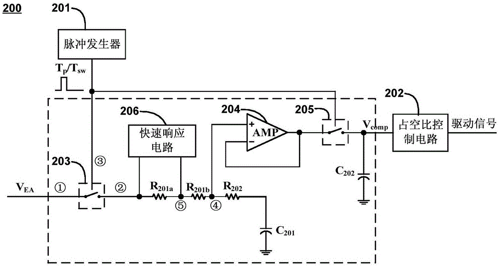
[0103] Figure 6 Shown is a simplified schematic diagram of the control part of the controller 200 integrated with the loop compensation circuit of the present invention in the secondary side feedback flyback converter, and image 3 Similarly, some circuits not related to loop control are omitted. Such as Figure 6 shown, the input voltage V IN The positive pole of the transformer passes through the primary winding N of the transformer P It is connected to the drain of the main power switch SW, and the source of the main power switch SW passes through the resistor RCS with input voltage V IN The negative pole of the main power switch tube SW is also connected to the current sensing pin of the controller 200, and the gate of the main power switch tube SW is connected to the drive signal output by the controller 200; the transformer secondary winding N S The anode and cathode of the rectifier diode D are connected in parallel to the output capacitor C OUT across the output ...
PUM
 Abstract
Description
Claims
Application Information