Quick controllable manufacturing method of large-area micron/nanometer texture on metal material surface
A metal material and nano-texture technology, applied in the direction of manufacturing tools, metal processing equipment, accessory devices, etc., can solve the problems of prolonging the process cycle and material waste, and achieve the effects of avoiding expensive prices, reducing processing costs, and shortening the processing cycle
- Summary
- Abstract
- Description
- Claims
- Application Information
AI Technical Summary
Problems solved by technology
Method used
Image
Examples
Embodiment 1
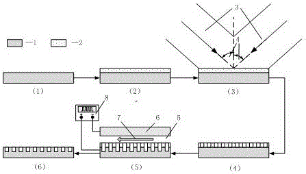
[0024] A controllable manufacturing method of a large-area micro-texture on the surface of a metal material of the present invention, such as figure 1 As shown, it can be divided into two parts: laser interference lithography and micro electrolytic processing, which specifically includes the following steps.
[0025] (1) Substrate pretreatment. The material of the substrate 1 is 304 stainless steel, which is ultrasonically cleaned in acetone, alcohol and deionized water for 5 minutes to remove oil stains and other dust impurities on the surface. Then, place it in a vacuum drying oven at 150° C. and bake for 10 minutes to ensure that its surface is relatively dry, which is beneficial to better bonding of the photoresist 2 and the surface of the substrate 1 .
[0026] (2) Gluing and pre-baking. The positive photoresist model AR-P3740 was selected, and the photoresist 2 was uniformly coated on the surface of the substrate 1 at a speed of 4000 rpm by using a high-speed coater, a...
Embodiment 2
[0032] (1) Substrate pretreatment. The material of the substrate 1 is TC1 titanium alloy, which is ultrasonically cleaned in acetone, alcohol and deionized water for 5 minutes to remove oil stains and other dust impurities on the surface. Then, place it in a vacuum drying oven at 150° C. and bake for 10 minutes to ensure that its surface is relatively dry, which is beneficial to better bonding of the photoresist 2 and the surface of the substrate 1 .
[0033](2) Gluing and pre-baking. The positive photoresist model AR-P3740 was selected, and the photoresist 2 was uniformly coated on the surface of the substrate 1 at a speed of 4000 rpm by using a high-speed coater, and the thickness of the obtained film was 1.4 μm. Then, the substrate 1 was pre-baked on a hot plate at 100° C. for 1 min.
[0034] (3) Interference exposure. The laser is an ultraviolet laser with a wavelength of 365nm, the incident angle is adjusted to 30°, and the exposure is set to 80mJ / cm 2 , the substrate...
Embodiment 3
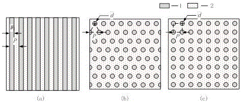
[0039] The preparation steps are the same as in Example 2. In step 3), the three-beam laser is replaced by a four-beam laser. The photoresist film pattern on the surface of the substrate after development is shown in figure 2 (c) shown.
PUM
 Abstract
Description
Claims
Application Information

