Semiconductor component, manufacturing method thereof and operating method thereof

A technology of semiconductors and oxide semiconductors, which is applied in semiconductor/solid-state device manufacturing, semiconductor devices, electrical components, etc., can solve the problems of insensitive clamping characteristics of HV-JFET, and achieve increased current, increased gate voltage, and leakage The effect of increasing pole current

Active Publication Date: 2015-11-25
MACRONIX INT CO LTD
View PDF6 Cites 4 Cited by
  • Summary
  • Abstract
  • Description
  • Claims
  • Application Information

AI Technical Summary

Problems solved by technology

However, HV-JFET requires a larger drift region (driftregion) area to form a Reduced Surface Field (RESURF), and the pinchoff (pinchoff) characteristics of HV-JFET are also less sensitive

Method used


Image

  • Semiconductor component, manufacturing method thereof and operating method thereof
  • Semiconductor component, manufacturing method thereof and operating method thereof
  • Semiconductor component, manufacturing method thereof and operating method thereof

Examples


Embodiment Construction

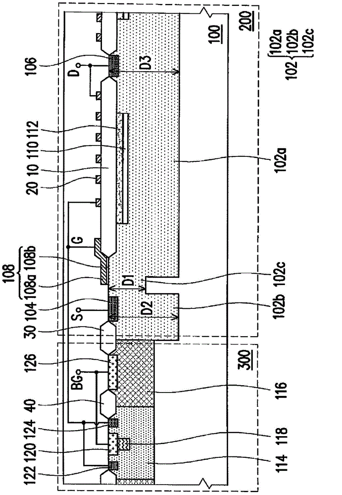
[0061] In the following embodiments, when the first conductivity type is N type, the second conductivity type is P type; when the first conductivity type is P type, the second conductivity type is N type. The P-type dopant is, for example, boron; the N-type dopant, for example, is phosphorus or arsenic. In this embodiment, the first conductivity type is N-type and the second conductivity type is P-type as an example for illustration, but the present invention is not limited thereto. In addition, the same or similar element symbols represent the same or similar elements.

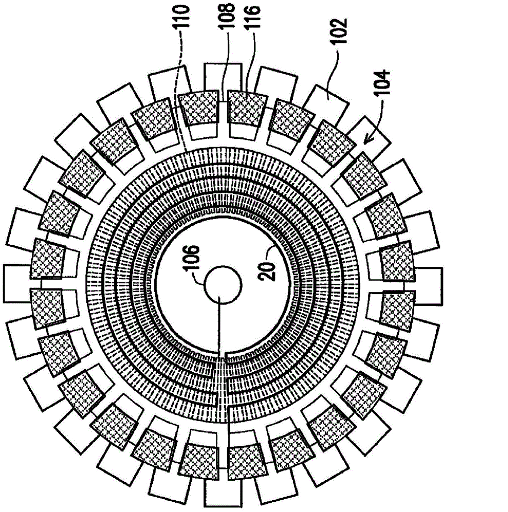
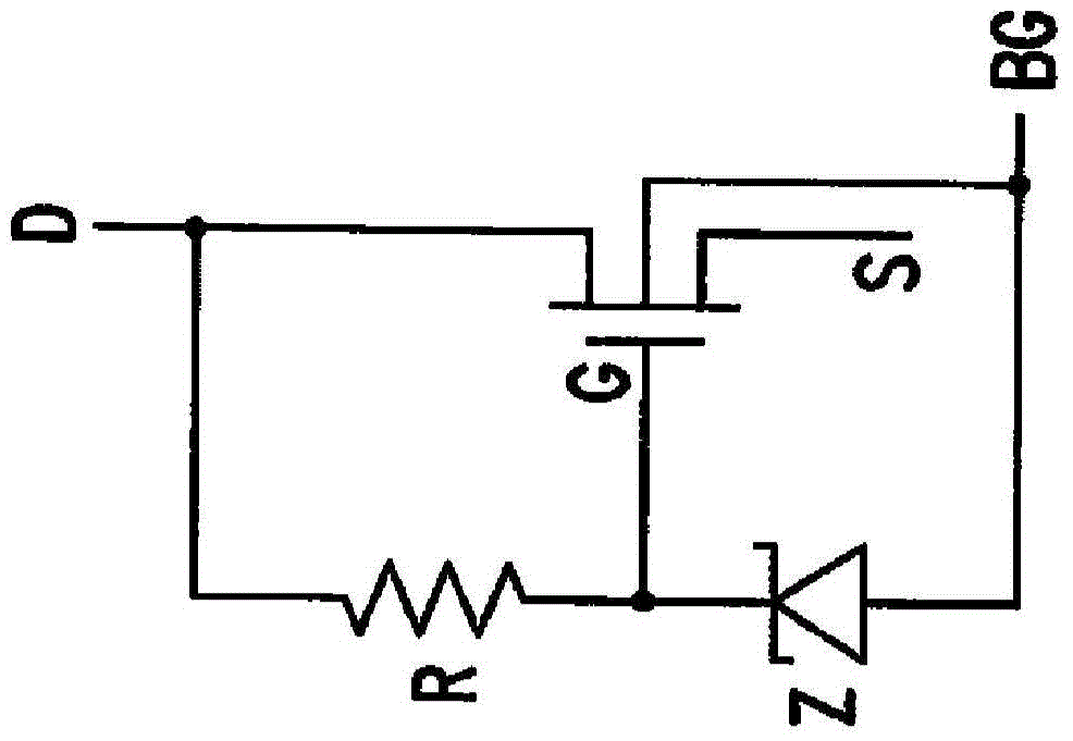
[0062] Figure 1A It is a schematic cross-sectional view of the semiconductor device of the first embodiment of the present invention. Figure 1B for Figure 1A top view of a semiconductor component. Please refer to Figure 1A , The semiconductor device of the first embodiment of the present invention includes: a metal oxide semiconductor transistor 200 , a Zener diode 300 and a high-resistance conductor st...


PUM


Abstract

The invention discloses a semiconductor component, a manufacturing method thereof and an operating method thereof. The semiconductor component includes a metal oxide semiconductor transistor, a resistor and a Zener diode. The metal oxide semiconductor transistor includes a grid electrode, a source electrode and a drain electrode. One end of the resistor is electrically connected with the drain electrode, and the resistor has a resistance value high enough to enable most current to flow through the metal oxide semiconductor transistor. The Zener diode includes a cathode and an anode, the cathode is electrically connected with the grid electrode and the other end of the resistor, and the anode is electrically connected with a grid electrode of a substrate.

Description

technical field [0001] The present invention relates to a semiconductor component, and in particular to a high-voltage semiconductor component, its manufacturing method and its operating method. Background technique [0002] The high-voltage device technology is widely used in power management integrated circuits (Power Management IC, PMIC), switching mode power supply (switching mode power supply, SMPS) and light emitting diode (light emitting diode, LED) driver. In recent years, with the rising awareness of environmental protection, the demand for green energy with high conversion efficiency and low standby power consumption has gradually attracted attention, making LEDs widely used in lighting. Generally speaking, LED drivers can be divided into linear LED drivers (Linear LED driver) and switch mode LED drivers (Switchmode LED driver). [0003] The high-voltage linear LED circuit uses a high-voltage depletion-type metal-oxide-semiconductor (HighVoltageDepletionMOS, HV-DM...

Claims


Application Information

Patent Timeline
Patent Type & Authority Applications(China)
IPC IPC(8): H01L27/06H01L21/8249
Inventor 陈永初
Owner MACRONIX INT CO LTD
Why Eureka
Try Eureka