Growth method for light-emitting diode epitaxial wafer and epitaxial wafer

A technology of light-emitting diodes and growth methods, which is applied to the growth method of light-emitting diode epitaxial wafers and the field of epitaxial wafers, can solve the problems of limited LED luminous efficiency, and achieve the effects of being conducive to two-dimensional growth, improving incorporation efficiency, and improving efficiency

Active Publication Date: 2015-11-25
HC SEMITEK SUZHOU
View PDF4 Cites 11 Cited by
  • Summary
  • Abstract
  • Description
  • Claims
  • Application Information

AI Technical Summary

Problems solved by technology

[0006] In order to solve the problem of limited luminous efficiency of LEDs in the prior art, an embodiment of the present invention provides a method for growing an epitaxial wafer of a light emitting diode and an epitaxial wafer

Method used


Image

  • Growth method for light-emitting diode epitaxial wafer and epitaxial wafer
  • Growth method for light-emitting diode epitaxial wafer and epitaxial wafer

Examples


Embodiment 1

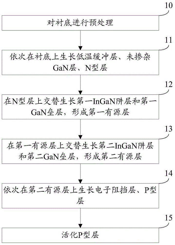
[0030] Embodiments of the present invention provide a method for growing light-emitting diode epitaxial wafers, see figure 1 , the growth method includes:

[0031] Step 10: pretreating the substrate. This step 10 is an optional step.

[0032] Alternatively, the substrate can be sapphire.

[0033] Specifically, this step 10 may include:

[0034] Under the hydrogen atmosphere, the substrate was treated at high temperature for 5-8 minutes. Wherein, the temperature of the reaction chamber can be 1000-1100° C., and the pressure of the reaction chamber can be controlled at 200-500 torr.

[0035] Step 11: growing a low-temperature buffer layer, an undoped GaN layer, and an N-type layer on the substrate in sequence.

[0036] In this embodiment, a VeecoK465i / C4MOCVD (MetalOrganicChemicalVaporDeposition, MetalOrganic Chemical VaporDeposition) equipment is used to realize the growth method of LED epitaxial wafers. Using high-purity H 2 (hydrogen) or high-purity N 2 (Nitrogen) or ...

Embodiment 2

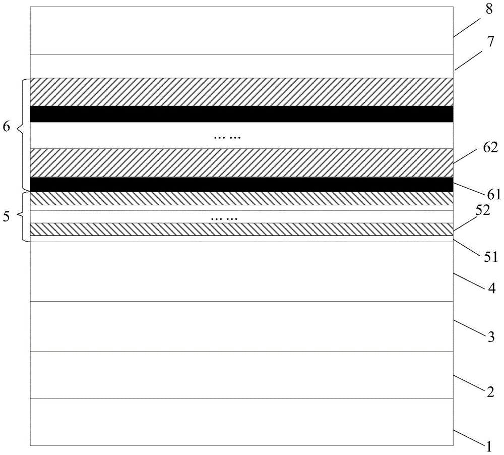
[0078] An embodiment of the present invention provides a light emitting diode epitaxial wafer, the light emitting diode epitaxial wafer is obtained by the growth method of the light emitting diode epitaxial wafer provided in the first embodiment, see figure 2 , the light-emitting diode epitaxial wafer includes a substrate 1, and a low-temperature buffer layer 2, an undoped GaN layer 3, an N-type layer 4, a first active layer 5, and a second active layer 6 sequentially stacked on the substrate 1 , the electron blocking layer 7, and the P-type layer 8.

[0079] In this embodiment, the first active layer 5 is formed of alternately grown first InGaN well layers 51 and first GaN barrier layers 52 . The second active layer 6 is formed of alternately grown second InGaN well layers 61 and second GaN barrier layers 62 .

[0080] Wherein, the growth pressure of the second active layer 6 is lower than the growth pressure of the first active layer 5, the growth speed of the second activ...


PUM


Abstract

The invention discloses a growth method for a light-emitting diode epitaxial wafer and an epitaxial wafer, belonging to the technical field of a semiconductor. The growth method comprises the following steps of: sequentially growing a low-temperature buffer layer, a non-doped GaN layer and an N-type layer on a substrate; alternatively growing a first InGaN pit layer and a first GaN barrier layer on the N-type layer to form a first active layer; alternatively growing a second InGaN pit layer and a second GaN barrier layer on the first active layer to form a second active layer; and sequentially growing an electron blocking layer and a P-type layer on the second active layer, wherein the growth pressure of the second active layer is lower than the growth pressure of the first active layer, the growth speed of the second active layer is lower than the growth speed of the first active layer, the thickness of the second active layer is smaller than the thickness of the first active layer, and the growth pressure, the growth speed and the thickness of the second InGaN pit layer are gradually reduced, slowed and decreased along the growth direction of the light-emitting diode epitaxial wafer. The epitaxial wafer is high in luminous efficiency.

Description

technical field [0001] The invention relates to the technical field of semiconductors, in particular to a growth method of a light-emitting diode epitaxial wafer and the epitaxial wafer. Background technique [0002] LED (LightEmittingDiode, light-emitting diode) is a semiconductor electronic component that can emit light. As an efficient, environmentally friendly, and green new solid-state lighting source, LEDs are being rapidly and widely used, such as traffic lights, automotive interior and exterior lights, urban landscape lighting, and mobile phone backlights. [0003] Epitaxial wafers are an important component in the manufacture of LEDs. The existing epitaxial growth method includes: sequentially growing a low-temperature buffer layer, an undoped GaN layer, an N-type layer, an active layer, and a P-type layer on a substrate. Wherein, the active layer is formed by alternately growing InGaN layers and GaN layers. [0004] In the process of realizing the present invent...

Claims


Application Information

Patent Timeline
Patent Type & Authority Applications(China)
IPC IPC(8): H01L33/00
CPCH01L33/0075
Inventor 姚振从颖陈柏松胡加辉魏世祯
Owner HC SEMITEK SUZHOU
Why Eureka
Try Eureka