
Composite machining method for micro-die

A composite processing and micro-mold technology, applied in the field of micro-processing, can solve the problems of expensive machine tools for processing micron-level feature sizes, affecting product bonding, sealing and testing, and the small size can only reach hundreds of nanometers, so as to shorten the preparation cycle , improve the service life, improve the effect of production efficiency

Active Publication Date: 2015-12-02
苏州含光微纳科技有限公司
View PDF6 Cites 3 Cited by
  • Summary
  • Abstract
  • Description
  • Claims
  • Application Information

AI Technical Summary

Problems solved by technology

However, due to the limitations of electroforming materials, the micro-mold materials prepared by this method are mainly copper and nickel. At the same time, due to the limitations of the electroforming process itself and the non-uniform distribution of the electric field, the structure obtained by electroforming is compared with that of thermally processed metals. The body material is more loose, and it is difficult to avoid defects such as voids
[0006] 3. Precision machining, mechanical cutting can obtain high-quality processed surfaces, and its roughness can reach several nanometers, but compared with plasma etching and quasi-LIGA technology based on photolithography, the feature size of precision machining Limited and extremely expensive machine tools for processing micron-scale feature sizes, while processing efficiency is very low
Among them, the preparation of micro-tool electrodes is the key. According to reports, micro-EDM technology based on tungsten-etched electrodes can prepare micro-molds with complex shapes. At the same time, this method can solve the feature size limitations and R in precision machining. corner problem, reduce the R corner radius to the micron level, but since the surface of the micro-EDM is composed of numerous electric erosion small pits, the minimum surface roughness can only reach a hundred nanometer level, for the subsequent use of the mold molding products , such as microfluidic chips, higher surface roughness will seriously affect the bonding and testing of products

Method used


Image

  • Composite machining method for micro-die
  • Composite machining method for micro-die
  • Composite machining method for micro-die

Examples


Embodiment Construction

[0037] In order to make the above objects, features and advantages of the present invention more obvious and understandable, the present invention will be further described below through specific embodiments and accompanying drawings.

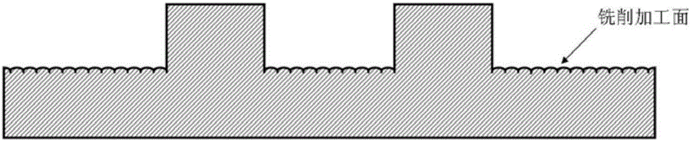
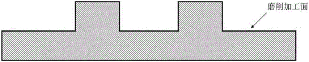
[0038] Taking the microfluidic chip mold as an example, the microfluidic chip is a basic network connected to micropumps, microreservoirs, microelectrodes, microdetection elements and other components with optical, electrical and fluid transport functions through microchannels. The functions of sampling, dilution, reaction, separation and detection are integrated on a microchip to the maximum extent, which has the advantages of small consumption of samples, fast and efficient biological reaction, etc., and is widely used in biomedical research, clinical diagnosis, judicial diagnosis and other fields. For a microfluidic chip, the width and depth of the microchannel are on the order of microns, while the size of the chip is usually on the order of...


PUM


Abstract

The invention relates to a composite machining method for a micro-die. According to the method, a mechanical cutting mode is adopted in a peripheral area of a graph of the micro-die for removing unnecessary materials and defining the outline of the graph area, and the high-quality machining surface is obtained; for the graph area of the micro-die, a tungsten tool electrode prepared through a plasma etching technology is utilized, a micro electrical discharge machining mode is adopted, accurate graph transferring is achieved, and machining precision and efficiency are ensured. According to the method, the technological advantage of precision machining and the technological advantage of micro electrical discharge machining are combined, the mechanical cutting mode is adopted for removing the unnecessary materials of the periphery of the graph of the micro-die, the electrical discharge area of follow-up micro electrical discharge machining can be reduced, aggregation of excessive electrically-corroded products is avoided, the stability of the electrical discharge process is improved, and the size precision and the surface quality of micro electrical discharge machining are ensured; meanwhile, the electrical discharge area is reduced, time for micro electrical discharge machining can be shortened, the machining efficiency is improved, and the requirement for the fast market response can be met.

Description

technical field [0001] The invention belongs to the technical field of micro-processing, and in particular relates to a composite processing method of a micro-mold. Background technique [0002] With the development of modern science and technology, miniaturization has become the main trend of product development. At present, the semiconductor industry, optical fiber communication, aerospace, bioengineering, and medical industries have more and more demands for micro-miniature products, and the requirements for the complexity and reliability of their structures and functions are also getting higher and higher. Therefore, making micro-molds through micro-processing technology, and then forming tiny products from micro-molds has the advantages of mass production, economy and reliability, and is an important development direction for large-scale production of micro-miniature products. [0003] Among them, the micro-mold is the core of the technology, and its surface roughness ...

Claims


Application Information

Patent Timeline
IPC IPC(8): B23H5/04
Inventor 陈兢陈献宋璐
Owner 苏州含光微纳科技有限公司
Learn More