Method of manufacturing back contact heterojunction single crystalline silicon solar cell

A technology of solar cells and monocrystalline silicon, applied in the field of solar photovoltaics, to achieve the effects of overcoming technical barriers, low cost, and simple process routes

Inactive Publication Date: 2015-12-02
深圳市科纳能薄膜科技有限公司
View PDF3 Cites 23 Cited by
  • Summary
  • Abstract
  • Description
  • Claims
  • Application Information

AI Technical Summary

Problems solved by technology

However, the difficult problem of electroplating technology is how to electroplate and form a metal film on the P-type and N-type amorphous silicon patterns, and effectively separate the positive and negative electrodes to avoid short circuit

Method used


Image

  • Method of manufacturing back contact heterojunction single crystalline silicon solar cell
  • Method of manufacturing back contact heterojunction single crystalline silicon solar cell
  • Method of manufacturing back contact heterojunction single crystalline silicon solar cell

Examples


Embodiment 1

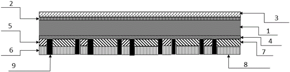
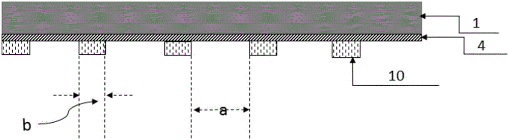
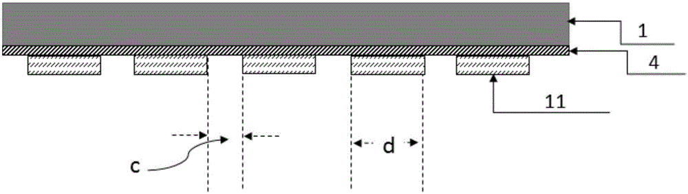
[0081]The structure of the back contact heterojunction solar cell prepared by the three-layer mask coating technology and electroplating technology provided in this example is as follows: figure 1 shown, including the following steps:

[0082] (1) Single crystal silicon cleaning, damage removal, texturing

[0083] Select an N-type monocrystalline silicon substrate with a resistivity of 0.5-50 Ω cm and a thickness of 50-500 μm for cleaning, removing the damaged layer, and making texture, which consists of the following steps:

[0084] Cleaning before texturing->remove surface damage of silicon wafer before texturing->texturing silicon wafer->cleaning after texturing->drying

[0085] The sliced ​​wafers were placed in CH 2 In the COOH organic solution, O is passed through the solution 3 , by ultrasonic cleaning. Immediately put the silicon wafer into 20% NaOH alkali solution after cleaning, and corrode it at 78°C for 0.5-1 minute, with an etching rate of 6-10 μm / min, to achi...

Embodiment 2

[0103] The structure of the back contact heterojunction solar cell prepared by the three-layer mask coating technology and electroplating technology provided in this example is as follows: figure 1 shown, including the following steps:

[0104] 1) Monocrystalline silicon cleaning, damage removal, texturing

[0105] Select a P-type monocrystalline silicon substrate with a resistivity of 0.5-50 Ω cm and a thickness of 50-500 μm for cleaning, removing the damaged layer, and making texture, which consists of the following steps:

[0106] Cleaning before texturing->remove surface damage of silicon wafer before texturing->texturing silicon wafer->cleaning after texturing->drying

[0107] The sliced ​​wafers were placed in CH 2 In the COOH organic solution, O3 was introduced into the solution and cleaned by ultrasonic waves. Immediately put the silicon wafer into 20% NaOH alkali solution after cleaning, and corrode it at 78°C for 0.5-1 minute, with an etching rate of 6-10 μm / min, ...


PUM

PropertyMeasurementUnit
thicknessaaaaaaaaaa
thicknessaaaaaaaaaa
thicknessaaaaaaaaaa

Abstract

The invention provides a method of manufacturing a back contact heterojunction single crystalline silicon solar cell, which belongs to the technical field of solar photovoltaics. The method comprises the following steps: (1) cleaning of single crystalline silicon, removal of a damage layer and etching are carried out; (2) a single crystalline silicon front surface passivation layer is formed, and coating of an anti-reflective layer is carried out; (3) coating of a single crystalline silicon back surface passivation layer is carried out; (4) a mask technology is adopted to form a P-type amorphous silicon pattern through coating of the single crystalline silicon back surface; (5) a mask technology is adopted to form an N-type amorphous silicon pattern through coating of the single crystalline silicon back surface; (6) a mask technology is adopted to form a protection film pattern through coating of the back surface; and (7) a chemical plating plus electroplating technology is adopted to form a contact electrode for a transmitting electrode and a base electrode on the back surface. the method of the invention has the advantages of simple process and low manufacturing cost whether for coating and positioning of a P / N junction or for back electrode manufacturing, and can be applied to mass production of the back contact heterojunction single crystalline silicon solar cells.

Description

technical field [0001] The invention belongs to the technical field of solar photovoltaics, and in particular relates to a method for manufacturing a back-contact heterojunction single-crystal silicon solar cell. Background technique [0002] Back contact technology and heterojunction technology are respectively a monocrystalline silicon solar cell technology that can achieve high conversion efficiency. In the back-contact solar cell, there is no electrode distribution on the front of the cell, and the emitter and base are cross-arranged on the back of the cell to respectively collect the photogenerated carriers generated by the photovoltaic effect of crystalline silicon. The loss can effectively increase the short-circuit current of the cell and greatly improve the conversion efficiency. In heterojunction solar cells, a layer of intrinsic amorphous silicon is inserted between the P-type amorphous silicon or N-type amorphous silicon and the single-crystal silicon substrate,...

Claims


Application Information

Patent Timeline
Patent Type & Authority Applications(China)
IPC IPC(8): H01L31/0216H01L31/0224H01L31/074H01L31/20
CPCH01L31/02167H01L31/022441H01L31/074H01L31/202Y02E10/50Y02P70/50
Inventor 张振刚萧生刚王海波赵崇亮
Owner 深圳市科纳能薄膜科技有限公司
Why Eureka
Try Eureka