Crystalline silicon solar cell and manufacture method thereof

A technology of solar cells and manufacturing methods, applied in the direction of circuits, photovoltaic power generation, electrical components, etc., can solve the problems of reduced electrical performance, reduced battery performance, reduced electrical performance, etc., to reduce contact area, reduce recombination loss, and reduce defect recombination Effect

Inactive Publication Date: 2015-12-02
SUZHOU TALESUN SOLAR TECH CO LTD
View PDF5 Cites 5 Cited by
  • Summary
  • Abstract
  • Description
  • Claims
  • Application Information

AI Technical Summary

Problems solved by technology

However, if the doping concentration of the silicon substrate is too high, many defects will be generated, the probability of recombination of photogenerated carriers in the highly doped region will increase, and the electrical properties will decrease. The similar heavily doped layer is called "dead layer".
In addition, the heavily doped surface has many defects, the surface recombination is serious, and the electrical performance is reduced.
That is to say, heavy doping is beneficial to the gold half-contact, but the performance of the battery is reduced

Method used


Image

  • Crystalline silicon solar cell and manufacture method thereof
  • Crystalline silicon solar cell and manufacture method thereof
  • Crystalline silicon solar cell and manufacture method thereof

Examples


Embodiment 1

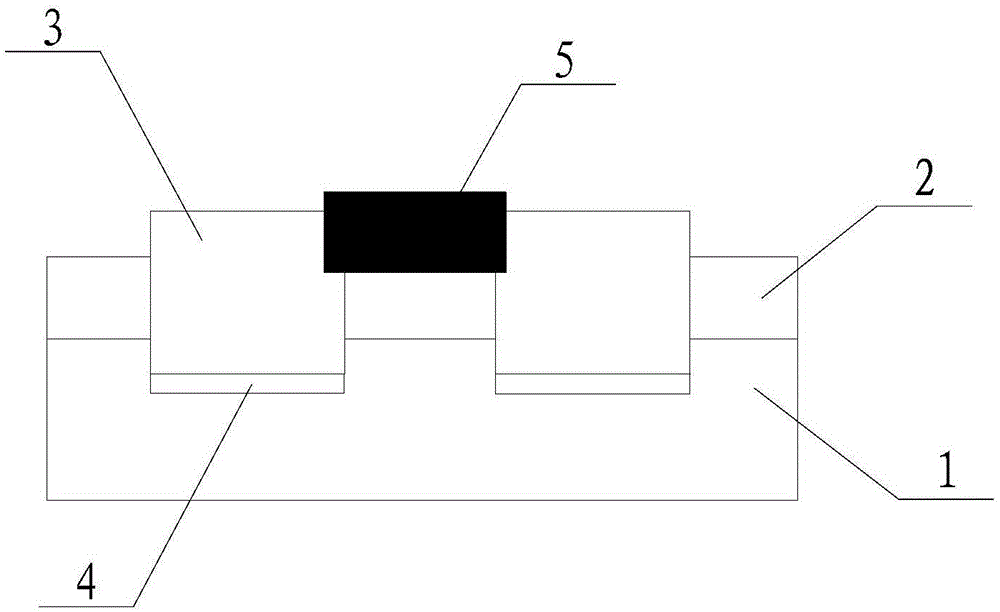
[0026] Such as figure 1 The crystalline silicon solar cell shown mainly includes an N-type silicon wafer substrate 1 , an antireflection film 2 , a first grid line 3 , a doped layer 4 and a second grid line 5 .

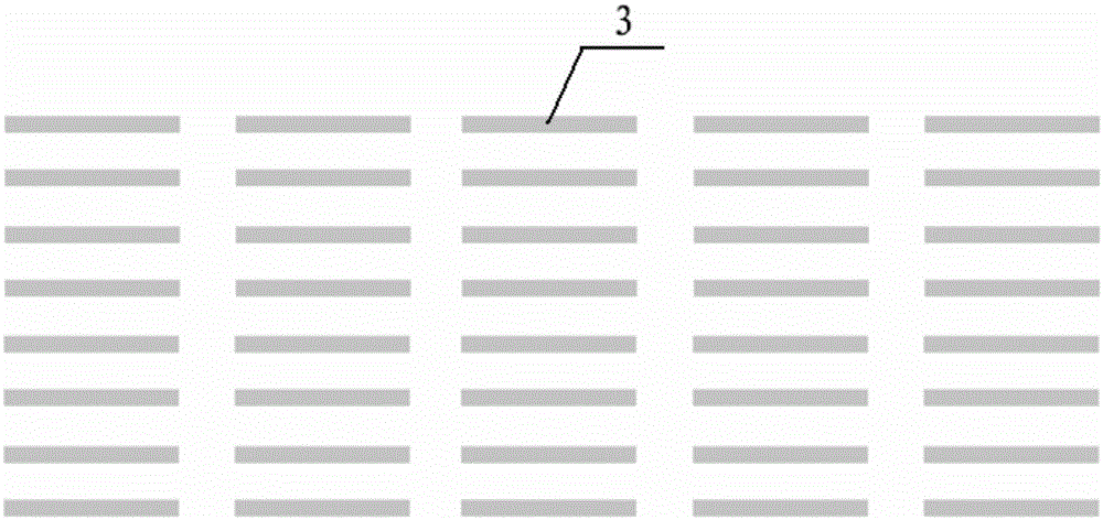
[0027] Wherein, the anti-reflection film 2 is formed on any surface of the N-type silicon wafer substrate 1 . There are multiple first grid lines 3, such as figure 2 As shown, they are arranged in multiple columns parallel to each other and arranged at intervals, and the corresponding first gate lines 3 in each column are on the same straight line; one end (bottom) of the first gate lines 3 is embedded in the N-type silicon substrate 1, the other end (upper part) extends beyond (or higher than) the anti-reflection film 2. The doped layer 4 is correspondingly formed on the bottom of the first gate line 3 and integrally formed on the surface of the N-type silicon substrate 1. The doped layer 4 is preferably a P heavily doped layer, so that the N-type silicon substrat...

Embodiment 2

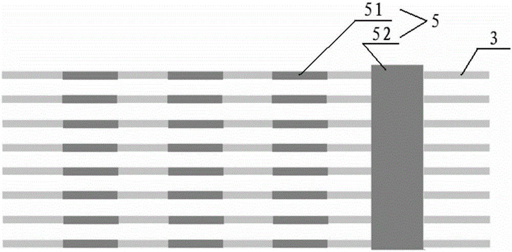
[0030] Such as Figure 4 The overall structure of the crystalline silicon solar cell shown is basically the same as that of the crystalline silicon solar cell in Embodiment 1, the difference is that the connecting grid lines 51 cover multiple first grid lines 3 on the same straight line, instead of only It is to connect opposite ends of two adjacent first grid lines 3 . The main gate line 52 covers the plurality of first gate lines 3 or the plurality of connecting gate lines 51 , and its extension direction is perpendicular to the extension direction of the corresponding first gate lines 3 in each column.

Embodiment 3

[0032] This embodiment provides a method for manufacturing a crystalline silicon solar cell in Embodiment 1, which includes the following steps:

[0033] (a) Form an antireflection film 2 on any surface of an N-type silicon wafer substrate 1. For the formation method, please refer to CN201510020649.4, specifically: adopt the lamination passivation method of aluminum oxide and silicon nitride, aluminum oxide It plays a passivation role, and silicon nitride plays the role of protecting and adjusting optical parameters and reducing reflectivity; the passivation anti-reflection film formed by aluminum oxide and silicon nitride can be produced by PECVD or ALD method, and the nitriding film can be produced by PECVD method Silicon passivation anti-reflection coating;

[0034] (b) Print the first paste corresponding to the first grid line 3 on the anti-reflection film 2, and dry it; the printing technology includes but not limited to screen printing, electroplating and 3D printing, et...


PUM


Abstract

The present invention relates to a crystalline silicon solar cell and a manufacture method thereof. The crystalline silicon solar cell includes a N type silicon wafer substrate; an antireflection film formed on any surface of the N type silicon wafer substrate; a plurality of first grid lines, wherein, one end of the first grid line is embedded in the N type silicon wafer substrate, and the other end of the first grid line extends and exceeds the antireflection film; a doping layer, wherein, the doping layer is correspondingly formed on the bottom of the first grid lines and integrates with the N type silicon wafer substrate; and a second grid line, wherein, the second grid line covers the first grid lines, is connected with the adjacent first grid line, and collects current. According to the above-mentioned method, a contact area of the grid lines and silicon is reduced, and a defect recombination due to contact is reduced, and furthermore, a recombination loss of heavy doping is reduced by the combination of silicon material partial doping, and a solar battery performance is increased.

Description

technical field [0001] The invention belongs to the field of photovoltaic solar cells, and in particular relates to a crystalline silicon solar cell and a manufacturing method thereof. Background technique [0002] Crystalline silicon solar cell is a photoelectric conversion device: an inverse doped layer is made on the silicon semiconductor substrate to form a PN junction, on which there is a surface passivation layer and an anti-reflection film, and the top layer is metallic silver (silver aluminum ) The grid wire draws the current, and after being illuminated, a continuous photogenerated current is generated. The manufacturing methods of the grid lines include screen printing, electroplating, and the like. This method of using metal grid lines as collectors for crystalline silicon cells is called metallization. [0003] The silicon in contact with the metal gate line requires as high a doping concentration as possible, heavy doping (1e 19 -1e 21 ) silicon can form ohm...

Claims


Application Information

Patent Timeline
Patent Type & Authority Applications(China)
IPC IPC(8): H01L31/0224
CPCH01L31/022433Y02E10/50
Inventor 倪志春魏青竹吴晨阳陆俊宇连维飞
Owner SUZHOU TALESUN SOLAR TECH CO LTD
Why Eureka
Try Eureka