Ultra-wideband artificial surface Plasmon low-pass filter

A technology of plasmonic polariton and low-pass filter, which is applied in the direction of waveguide devices, electrical components, circuits, etc., can solve the problem that the plasmonic waveguide structure cannot realize the high-efficiency conversion function of the microstrip line, and achieve good technical foresight and technical foresight Good, easy-to-manufacture effects

Inactive Publication Date: 2015-12-02
NANJING UNIV OF AERONAUTICS & ASTRONAUTICS
View PDF4 Cites 31 Cited by
  • Summary
  • Abstract
  • Description
  • Claims
  • Application Information

AI Technical Summary

Problems solved by technology

[0004] Technical problem: The technical problem to be solved by the present invention is to design a microstrip line with simple and symmetrical structure, compact size, and easy to use with traditional microwave transmission lines in view of the defect that the plasmonic waveguide structure cannot realize the high-efficiency conversion function of the traditional mic

Method used


Image

  • Ultra-wideband artificial surface Plasmon low-pass filter
  • Ultra-wideband artificial surface Plasmon low-pass filter
  • Ultra-wideband artificial surface Plasmon low-pass filter

Examples


Embodiment 1

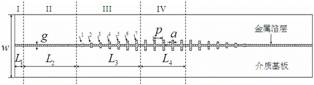
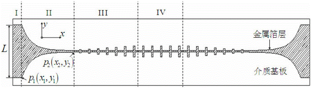
[0020] As shown in Fig. 1(a) and Fig. 1(b), the present invention includes a dielectric substrate layer and a metal foil layer printed on the upper and lower surfaces of the dielectric substrate. The waveguide structure is engraved on the metal foil layer, and the waveguide structure is mainly composed of the microstrip line part (area I) with both ends symmetrical, and the transition part (areas II and III) from the microstrip line structure with both ends symmetrical to the surface plasmon waveguide structure. And the intermediate surface plasmon waveguide part (region IV). Wherein, the microstrip line part includes a dielectric substrate layer, a metal central conduction strip and a metal grounding plate printed on the upper and lower surfaces of the substrate. The width of the metal ground plate is greater than the width of the metal central conductive strip. The transition part includes two transition stages. The first transition stage (region II) continues the metal cen...

Embodiment 2

[0022] Shown in Fig. 1 (a), Fig. 1 (b) is the front and back structural diagrams of the present invention, the horizontal total length of the present invention is 165 millimeters, and transverse width w=30 millimeters. The thickness of the metal foil layer is 0.018 mm, the thickness of the dielectric substrate is 0.254 mm, and the dielectric constant is 2.2. The total horizontal length of the part of area I is L 1 = 5 mm, wherein, the width of the metal center conduction band on the upper surface g = 0.75 mm, the lateral width of the ground plate on the lower surface L = 24 mm; the total horizontal length of the region II (the first transition stage on the left) is L 2 = 17.5 mm, where the metal center conduction band on the upper surface is consistent with the microstrip line, and the lateral width of the ground plate on the lower surface can be according to the Goubau curve Realize gradual change (note: the form of the curve is not unique, but it is necessary to ensure the...


PUM

PropertyMeasurementUnit
Thicknessaaaaaaaaaa
Thicknessaaaaaaaaaa
Dielectric constantaaaaaaaaaa

Abstract

The invention discloses an ultra-wideband artificial surface Plasmon low-pass filter which is mainly formed by a dielectric substrate layer and metallic foil layers printed on the both side surfaces of the dielectric substrate layer. Waveguide structures are engraved on the metallic foil layers. Each waveguide structure is formed by a middle surface Plasmon waveguide portion, symmetric microstrip line portions at both ends, and two transition portions. The ultra-wideband artificial surface Plasmon low-pass filter may achieve effective transmission of artificial surface Plasmon waveguide, and has symmetric structure, easy processing, compact size, a ultra-wide band and high filtering performance, and is especially suitable for being used in cooperation with a conventional microwave or terahertz transmission line.

Description

technical field [0001] The invention relates to a filter structure, in particular to an ultra-wideband artificial surface plasmon low-pass filter. Background technique [0002] A surface plasmon is a mixed excited state of electrons and photons that exists at the interface between a metal and a medium (usually air). It is essentially a surface electromagnetic wave, which can break through the diffraction limit. The electromagnetic field is confined in the sub-wavelength range near the interface between the metal and the medium, and has a strong field enhancement effect. This type of research was once limited to the optical band or higher frequencies. Due to the excellent characteristics of surface plasmons, if the concept of surface plasmons is extended to low frequency bands (microwave or terahertz bands), it will help Obtain guided wave technology for highly constrained microwave or terahertz signals, and reduce the size of low-frequency devices to sub-wavelength levels t...

Claims


Application Information

Patent Timeline
IPC IPC(8): H01P1/20H01P1/203
Inventor 刘亮亮李茁宁苹苹徐佳许秉正陈晨顾长青陈新蕾
Owner NANJING UNIV OF AERONAUTICS & ASTRONAUTICS
Why Eureka
Try Eureka