Eureka AIR delivers breakthrough ideas for toughest innovation challenges, trusted by R&D personnel around the world.

Gaas thin film grown on Si substrate and preparation method thereof

A substrate and thin film technology, applied in the field of GaAs thin films and their preparation, can solve the problems of deteriorating device performance, GaAs misfit dislocation, affecting the surface flatness of GaAs semiconductor devices, etc. GaAs epitaxy thin high quality effect

Active Publication Date: 2017-11-07
SOUTH CHINA UNIV OF TECH
View PDF4 Cites 0 Cited by
  • Summary
  • Abstract
  • Description
  • Claims
  • Application Information

AI Technical Summary

Problems solved by technology

On the one hand, the lattice constant of Si is smaller than that of GaAs, and there is more than 4% lattice mismatch between them, which will cause a large number of misfit dislocations in GaAs during growth, deteriorating device performance
On the other hand, due to the surface characteristics of the Si substrate, defects such as twin crystals and reverse domains are also more likely to appear, especially when there is a large mismatch stress between the epitaxial material and the substrate.
The formation of these defects will cause a large number of pyramid-shaped or trench-shaped protrusions to form on the surface of the epitaxial film, which seriously affects the surface flatness of GaAs semiconductor devices.

Method used

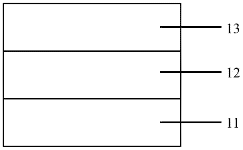
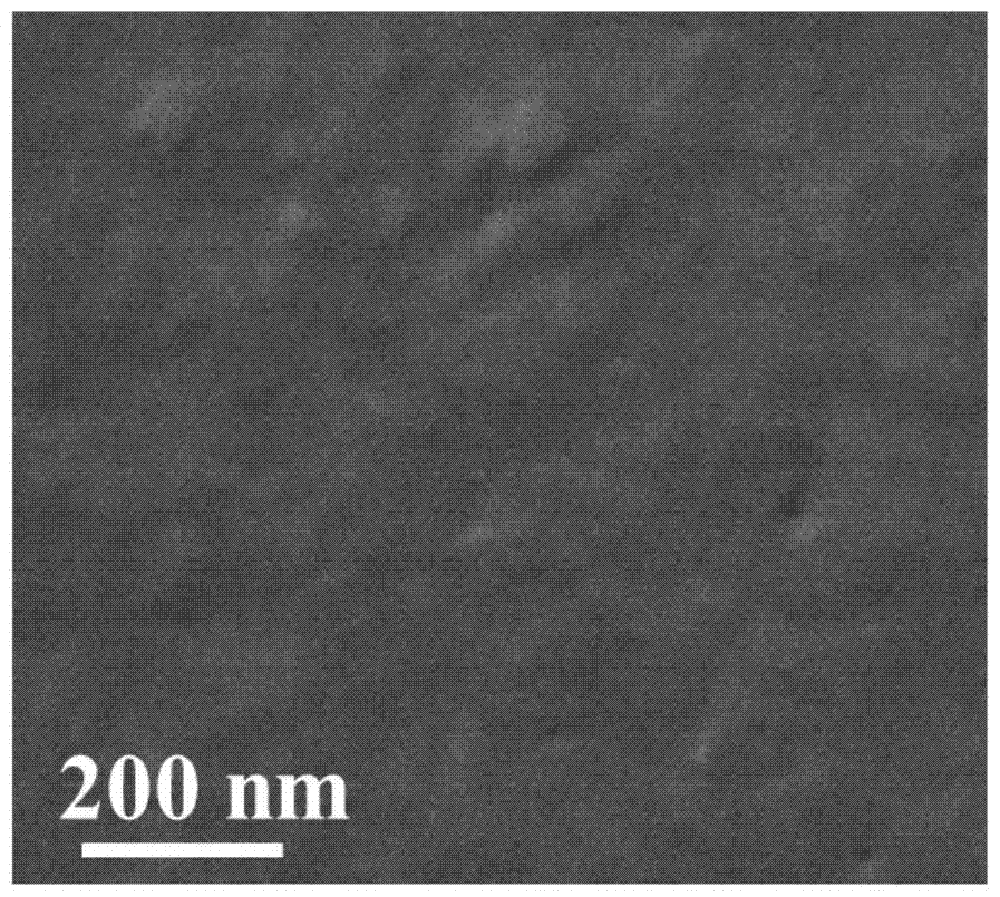
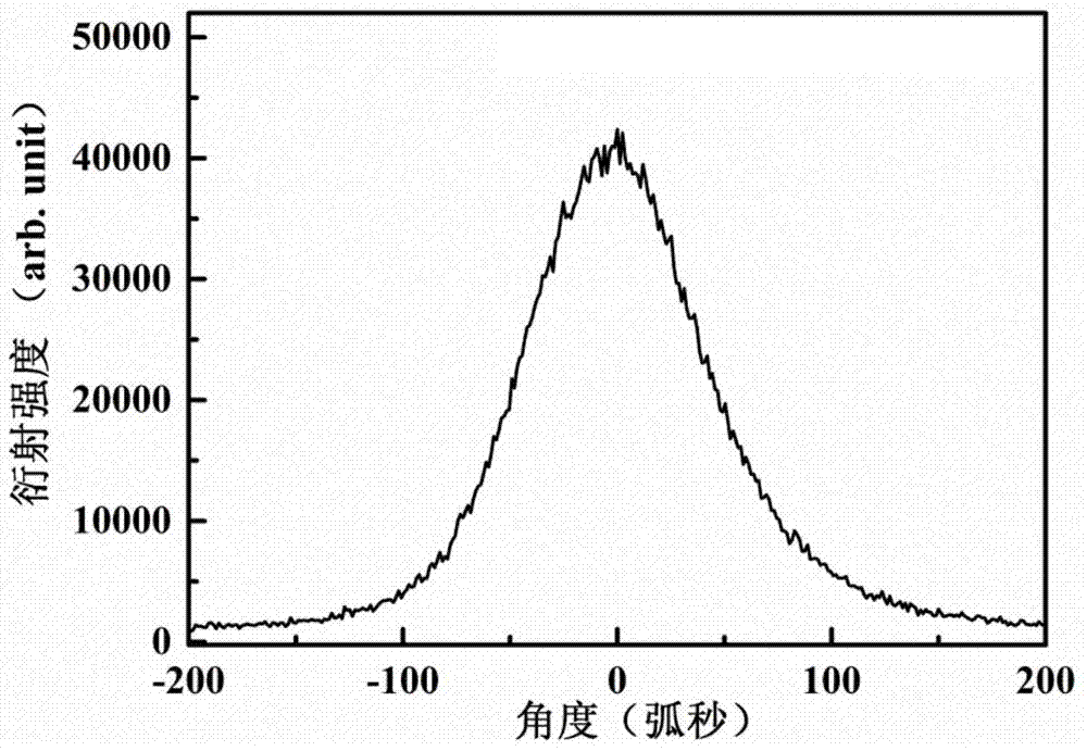

Image

  • Gaas thin film grown on Si substrate and preparation method thereof
  • Gaas thin film grown on Si substrate and preparation method thereof
  • Gaas thin film grown on Si substrate and preparation method thereof

Examples


Embodiment 1

[0037] The preparation method of the GaAs thin film grown on the Si substrate of the present embodiment comprises the following steps:

[0038] (1) Si substrate cleaning: After washing with acetone and deionized water, organic matter on the surface of the substrate is removed; the Si substrate is placed in HF:H 2 Ultrasound in O=1:10 solution for 1 minute, then rinse with deionized water to remove surface oxides and organic matter; dry the cleaned Si substrate with high-purity nitrogen;

[0039] (2) Si substrate pretreatment: After the Si substrate is cleaned, send it to the molecular beam epitaxy sampling chamber for pre-degassing for 15 minutes; then send it to the transfer chamber for degassing at 300°C for 0.5 hours, and then send it to the growth chamber after degassing;

[0040] (3) Si substrate deoxidation film: after the Si substrate enters the growth chamber, the substrate temperature is raised to 950 ° C, and the high temperature is baked for 15 minutes to remove the...

Embodiment 2

[0048] The preparation method of the GaAs thin film grown on the Si substrate of the present embodiment comprises the following steps:

[0049] (1) Si substrate cleaning: After washing with acetone and deionized water, organic matter on the surface of the substrate is removed; the Si substrate is placed in HF:H 2 Ultrasonic in O=1:10 solution for 10 minutes, then rinsed with deionized water to remove surface oxides and organic matter; the cleaned Si substrate was dried with high-purity nitrogen;

[0050] (2) Si substrate pretreatment: After the Si substrate is cleaned, it is sent to the molecular beam epitaxy sampling chamber for pre-degassing for 30 minutes; then sent to the transfer chamber for degassing at 400 °C for 2 hours, and then sent to the growth chamber after degassing;

[0051] (3) Si substrate deoxidation film: after the Si substrate enters the growth chamber, the temperature of the substrate is raised to 1050 ° C, and the high temperature is baked for 30 minutes ...


PUM

PropertyMeasurementUnit
thicknessaaaaaaaaaa

Abstract

The invention discloses a preparation method for a GaAs thin film grown on a Si substrate. The preparation method comprises the following steps of: (1) cleaning the Si substrate; (2) pre-processing the Si substrate; (3) deoxidizing the Si substrate; (4) growing a buffer layer, in which an In<x>Ga<1-x>P buffer layer of 2 to 20 nanometers is grown on the surface of the Si substrate processed through the step (3) at a growth temperature of 350-500 DEG C; and (5) growing the GaAs thin film, in which the GaAs thin film is grown on the In<x>Ga<1-x>P buffer layer at a growth temperature of 500-580 DEG C. The invention also discloses the GaAs thin film grown on the Si substrate. The preparation method has the advantages of simplicity in the structure of the buffer layer, convenience in an epitaxial growth process and the like, and the obtained GaAs epitaxial thin film is flat in surface, low in dislocation density and high in crystal quality.

Description

technical field [0001] The invention relates to a GaAs thin film and a preparation method thereof, in particular to a GaAs thin film grown on a Si substrate and a preparation method thereof. Background technique [0002] III-V compounds are widely used in optoelectronic devices due to their advantages of good stability, small effective mass, high electron mobility and peak velocity, and high light absorption coefficient. Among them, the band gap of GaAs is 1.42eV, which corresponds to the highest energy band in the solar spectrum, so it is very suitable for the production of solar cells and photodetectors. Commonly used substrate materials for growing GaAs semiconductor devices are GaAs or Ge, etc., but these materials are expensive, thus increasing the preparation cost of GaAs-based semiconductor materials. Compared with GaAs and Ge, Si has the advantages of mature technology, low price, and easy large-scale size. If epitaxial growth of high-quality GaAs materials can be r...

Claims


Application Information

Patent Timeline
Patent Type & Authority Patents(China)
IPC IPC(8): H01L21/02
CPCH01L21/02381H01L21/02461H01L21/02499H01L21/02546H01L21/02631
Inventor 李国强温雷高芳亮张曙光李景灵龚振远
Owner SOUTH CHINA UNIV OF TECH
Why Eureka
Eureka Blog
Learn More