Semiconductor device and manufacturing method thereof

A manufacturing method and semiconductor technology, applied in the field of microelectronics, can solve the problems of inability to dissipate heat and low withstand voltage, and achieve the effect of improving the withstand voltage and uniform temperature distribution

Inactive Publication Date: 2015-12-09
DYNAX SEMICON
View PDF3 Cites 13 Cited by
  • Summary
  • Abstract
  • Description
  • Claims
  • Application Information

AI Technical Summary

Problems solved by technology

[0006] The object of the present invention is to propose a semiconductor device and its manufacturing method, which can solve the problems of the heat inside the semiconductor device in the prior art that cannot be dissipated and the withstand voltage is low

Method used


Image

  • Semiconductor device and manufacturing method thereof
  • Semiconductor device and manufacturing method thereof
  • Semiconductor device and manufacturing method thereof

Examples


Embodiment 1

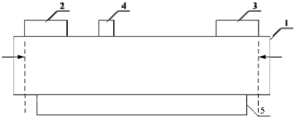
[0063] figure 1 is a cross-sectional view of the semiconductor device provided by Embodiment 1 of the present invention. like figure 1 As shown, the semiconductor device includes:

[0064] Semiconductor layer 1.

[0065] A source 2 and a drain 3 located on the semiconductor layer 1 , and a gate 4 located on the semiconductor layer 1 and between the source 2 and the drain 3 .

[0066] A thermally conductive and / or voltage resistant layer 5 is disposed below the semiconductor layer 1 .

[0067] Preferably, the semiconductor layer may include a buffer layer and a channel layer stacked sequentially from bottom to top.

[0068] Preferably, the channel layer may be a silicon carbide-based material, and the semiconductor device may be a silicon carbide device.

[0069] Preferably, the channel layer further includes a barrier layer, the barrier layer and the channel layer form a heterojunction structure, and a two-dimensional electron gas is formed at the interface of the heteroj...

Embodiment 2

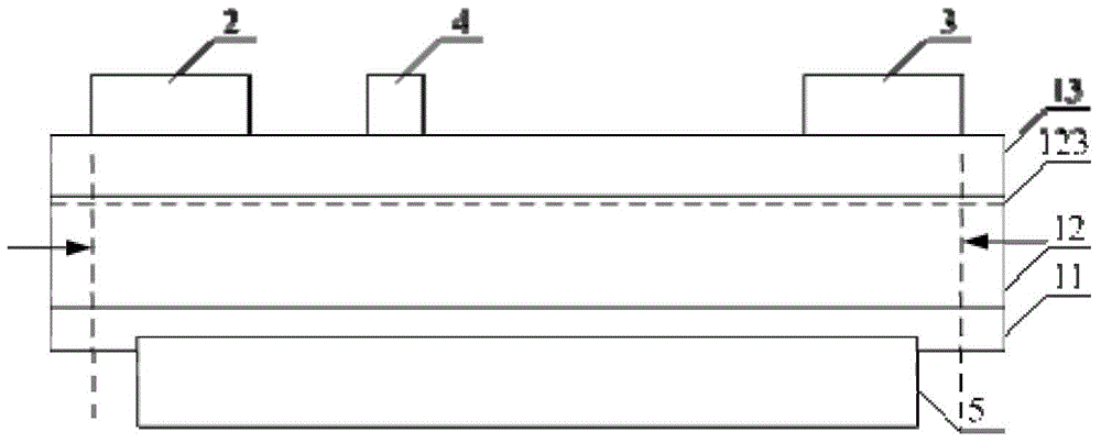
[0078] figure 2 It is a cross-sectional view of a gallium nitride semiconductor device provided in Embodiment 2 of the present invention. like figure 2 As shown, different from the semiconductor device provided in Embodiment 1 of the present invention, the semiconductor layer of the semiconductor device provided in Embodiment 2 includes from bottom to top: buffer layer 11, nitride channel layer 12 and nitride barrier layer 13. Among them, 123 is a two-dimensional electron gas. The thermally conductive and / or pressure-resistant layer 5 is disposed within the buffer layer 11 .

[0079] Wherein, the material of the buffer layer 11 can be group III nitrides such as aluminum gallium nitride, gallium nitride or aluminum indium gallium nitride; the material of the nitride channel layer 12 can be group III nitrides such as gallium nitride; the nitride barrier layer The material of 13 can be group III nitrides such as aluminum gallium nitride; the buffer layer can play the role o...

Embodiment 3

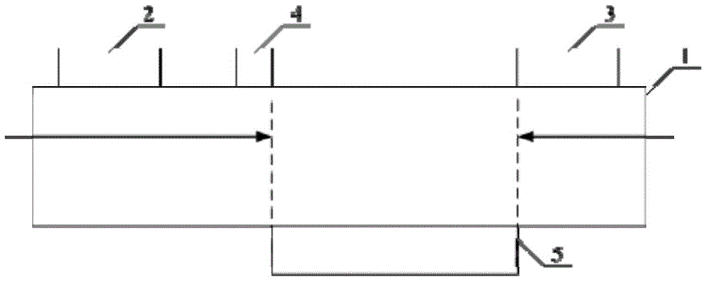
[0083] image 3 It is a cross-sectional view of the semiconductor device provided by Embodiment 3 of the present invention. like image 3 As shown, different from the semiconductor device provided in Embodiment 1 of the present invention, the heat conduction and / or voltage resistance layer 5 of the semiconductor device is located under the semiconductor layer 1 between the gate 4 and the drain 3 .

[0084] When a semiconductor device is in operation, the heat is mainly concentrated in the area between the gate and the drain. A thermally conductive and / or voltage-resistant layer is arranged under the semiconductor layer between the gate and the drain, and the area between the gate and the drain is formed by using the thermally conductive layer or the thermally conductive and voltage-resistant layer, as shown in the figure As shown in the range surrounded by the dotted line, most of the accumulated heat is dissipated effectively, uniformly and in a timely manner, making the te...


PUM


Abstract

The invention discloses a semiconductor device and a manufacturing method thereof. The semiconductor device comprises a semiconductor layer, a source and a drain disposed on the semiconductor layer, a gate disposed on the semiconductor layer and between the source and the drain, and a heat conduction and / or voltage-resistant layer disposed below and / or inside the semiconductor layer. According to the semiconductor device and the manufacturing method thereof provided by the embodiments of the invention, the heat conduction and / or voltage-resistant layer is disposed below and / or inside the semiconductor layer, and heat accumulated in a heat accumulation area (the area between the outer edge of the source and the outer edge of the drain) can be dissipated out effectively, uniformly and timely through the heat conduction layer or the heat conduction and voltage-resistant layer, so that the temperature inside the semiconductor device is uniformly distributed, and the withstand voltage of the semiconductor device can be improved. The withstand voltage of the semiconductor device is improved through the heat conduction layer or the heat conduction and voltage-resistant layer.

Description

technical field [0001] The invention relates to the technical field of microelectronics, in particular to a semiconductor device and a manufacturing method thereof. Background technique [0002] Gallium nitride and silicon carbide, wide bandgap compound semiconductor materials, have the characteristics of large bandgap width, high electron saturation drift velocity, high breakdown field strength, and good thermal conductivity. GaN high electron mobility devices, in particular, have attracted the attention of many researchers all over the world for their superior performance and huge development potential. [0003] Due to the high power density of wide bandgap compound (gallium nitride and silicon carbide) semiconductor devices, their heat density is also very high, resulting in very large heat generated by the device during operation. If the heat cannot be dissipated in time, it will be It will cause a high internal temperature of the device, affect the stability and reliab...

Claims


Application Information

Patent Timeline
Patent Type & Authority Applications(China)
IPC IPC(8): H01L29/78H01L29/778H01L21/336
CPCH01L29/78H01L29/66477H01L29/7786
Inventor 裴风丽裴轶张乃千
Owner DYNAX SEMICON
Why Eureka
Try Eureka