Surface covered tin‑nano tio 2 Membrane electronic device housing and method for processing the same

A surface covering and electronic device technology is applied to the electronic device casing and its processing field covered with a TiN-nano TiO2 film. The effect of reducing the growth or spread of bacteria and improving the competitiveness of products

Active Publication Date: 2017-12-12
大昶(重庆)电子科技有限公司
View PDF5 Cites 0 Cited by
  • Summary
  • Abstract
  • Description
  • Claims
  • Application Information

AI Technical Summary

Problems solved by technology

[0005] The purpose of the present invention is to provide surface covered TiN-nano TiO 2 The film electronic device casing and its processing method effectively solve the problem that the electronic device casing is easy to accumulate dust and be polluted, and provide an electronic device casing that is easy to clean and its processing method

Method used


Image

  • Surface covered tin‑nano tio  <sub>2</sub> Membrane electronic device housing and method for processing the same
  • Surface covered tin‑nano tio  <sub>2</sub> Membrane electronic device housing and method for processing the same

Examples


Embodiment 1

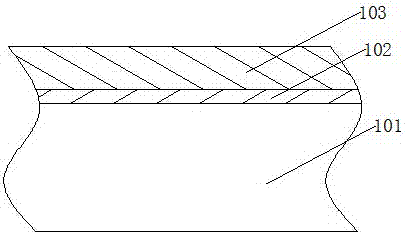
[0038] Surface covered with TiN-nano TiO 2 Film electronic device housing, such as figure 2 As shown, including the substrate and the nano TiO covering the outer surface of the substrate 2 Membrane 103 and connection matrix with nano TiO 2 The pre-layer of the film 103; the nano TiO 2 The film 103 is a rutile phase lattice structure or an anatase phase lattice structure or a mixed lattice structure of rutile phase and anatase phase, and its thickness is 20-80 nm; the substrate is a ceramic substrate 101, and the pre-layer is TiN The preset layer 102.

[0039] The surface provided by the invention is covered with TiN-nano TiO 2 The electronic device housing of the membrane does not interfere with electronic signals, and has the characteristics of easy cleaning and self-cleaning. Nano TiO 2 The film 103 can not only make the housing present a metallic appearance, but can also decompose dust, sweat or residual organic pollutants adhered to the surface of the housing under the irrad...

Embodiment 2

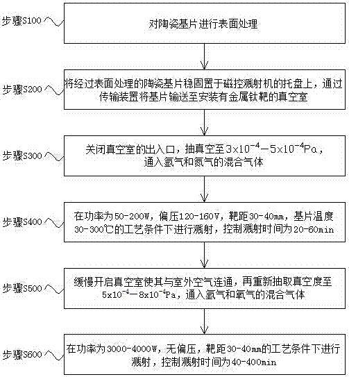
[0043] Surface covered with TiN-nano TiO 2 The processing method of the electronic device housing of the film, such as figure 1 As shown, including the following steps:

[0044] Step S100: performing surface treatment on the ceramic substrate 101;

[0045] Step S200: Place the surface-treated ceramic substrate 101 firmly on the tray of the magnetron sputtering machine, and transport the substrate to the vacuum chamber where the metal titanium target is installed through the transmission device;

[0046] Step S300: Close the entrance and exit of the vacuum chamber, and pump the vacuum to 3x10 -4 —5x10 -4 Pa, a mixed gas of argon and nitrogen;

[0047] Step S400: Sputtering is performed under the process conditions of a power of 50-200W, a bias voltage of 120-160V, a target distance of 30-40mm, and a substrate temperature of 30-300°C, and the sputtering time is controlled to be 20-60min;

[0048] Step S500: Slowly open the vacuum chamber to communicate with the outdoor air, and then re-ex...

Embodiment 3

[0052] This embodiment is further optimized on the basis of Embodiment 2. Further, the step S100 specifically refers to the following process:

[0053] Step S110: Put the ceramic substrate 101 in a water area with a water temperature of 60-80°C and let stand for 1-2 hours;

[0054] Step S120: Put the ceramic substrate 101 into a cleaning tank equipped with a 20-50% acetone solution, and use ultrasonic cleaning for 10-20 minutes;

[0055] Step S130: Rinse the ceramic substrate 101 with flowing deionized water to remove the acetone solution;

[0056] Step S140: Take out the ceramic substrate 101 and blow dry its surface with cold air, and set it aside. The other parts of this embodiment are the same as that of Embodiment 2, so they will not be repeated.


PUM

PropertyMeasurementUnit
thicknessaaaaaaaaaa

Abstract

The invention discloses an electronic device shell with the surface covered with a TiN-nanometer TiO<2> film and a processing method for the electronic device shell. A ceramic substrate (101) is firstly coated with a TiN film precoated layer (102) by adjusting process parameters by means of magnetron sputtering, and then the TiN film precoated layer (102) is firstly coated with a nanometer TiO<2> film (103), and the film is even. The problems of dust accumulation and contamination of an electronic device shell are solved, so that the electronic device shell has the characters of being easy to clean and achieving self cleaning, and product competitiveness is improved. In addition, in the processing process, the utilization rate of targets is high, and safety and environment friendliness are achieved.

Description

Technical field [0001] The invention relates to the field of electronic devices, in particular to the TiN-nano TiO surface covering 2 Film electronic device casing and processing method thereof. Background technique [0002] The casing of the existing electronic product is coated with a metal layer to avoid signal interference to obtain better operation strength and texture, but the metal layer does not have a cleaning function, and the surface is likely to accumulate dust, sweat, etc., which affects the use of the electronic product. [0003] Titanium dioxide film has a good photocatalytic effect, can decompose some organic matter under ultraviolet radiation, and has a certain self-cleaning ability. [0004] Magnetron sputtering deposition means that particles with sufficiently high energy bombard the surface of the target material, so that the atoms in the target material obtain enough energy through collision to emit from the surface, and then change the direction of movement of t...

Claims


Application Information

Patent Timeline
Patent Type & Authority Patents(China)
IPC IPC(8): C23C14/35C23C14/08C23C14/02H05K5/02
CPCC23C14/0036C23C14/021C23C14/024C23C14/0641C23C14/083C23C14/35H05K5/02
Inventor 鲍必辉
Owner 大昶(重庆)电子科技有限公司
Why Eureka
Try Eureka