High-detective-efficiency single photon avalanche diode detector array unit

A single-photon avalanche, detector array technology, applied in electrical components, semiconductor devices, circuits, etc., can solve the problems of low detection efficiency, low photon detection efficiency, etc., to improve detection efficiency, improve photon detection efficiency, and increase depth. Effect

Active Publication Date: 2015-12-23
NANJING UNIV OF POSTS & TELECOMM INST AT NANJING CO LTD
View PDF2 Cites 40 Cited by
  • Summary
  • Abstract
  • Description
  • Claims
  • Application Information

AI Technical Summary

Problems solved by technology

[0005] The object of the present invention is to solve the problem of low detection efficiency of traditional SPAD detectors, and proposes a single photon avalanche diode detector array u

Method used


Image

  • High-detective-efficiency single photon avalanche diode detector array unit
  • High-detective-efficiency single photon avalanche diode detector array unit
  • High-detective-efficiency single photon avalanche diode detector array unit

Examples


Embodiment Construction

[0027] The invention will be described in further detail below in conjunction with the accompanying drawings.

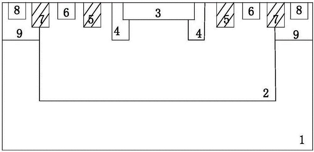
[0028] Such as figure 1As shown, it is a cross-sectional schematic diagram of a traditional SPAD array unit; the active region of the array unit includes a P-type substrate 1; a deep N well 2; a P+ region 3; a P well 4 inside the deep N well; a P well and a P+ region The shallow trench isolation (STI) region 5 between them; the N+ region 6; the shallow trench isolation (STI) region 7 between the two P+ regions; the P+ region 8; the P wells 9 on both sides of the P-type substrate. There is a deep N well 2 in the P-type substrate 1 of the traditional SPAD structure. The center of the surface of the deep N well 2 is a P+ region 3. The electrode on the surface of this region is used as the anode of the SPAD device. In the avalanche region, the lightly doped P well 4 surrounded by the P+ region 3 can prevent edge breakdown and edge effects. Both sides of the upper surfa...


PUM


Abstract

The invention discloses a high-detective-efficiency single photon avalanche diode (SPAD) detector array unit. The array unit adopts a surrounded type SPAD structure with a deep P well protected by a P-injection layer, a P buried layer and a P-buried layer, i.e., the deep P well is formed in a P type substrate through ion injection, two buried layer regions, i.e., a P buried layer region 3 and a P-buried layer region 4, are arranged in the deep P well, and the upper part of the P-buried layer region 4 is surrounded by a P-injection region 8. The structure of the array unit can effectively improve the photon detection efficiency of an SPAD device, and the dark count rate is very low, so that the overall performance of an SPAD detector is improved very well.

Description

technical field [0001] The invention relates to a single-photon avalanche photodiode detector array unit with high detection efficiency, which belongs to the field of optoelectronic technology. Background technique [0002] Single-photon avalanche photodiode (ie: SPAD) has the characteristics of fast response speed, large avalanche gain, high detection efficiency, small size, light weight, and low power consumption, so it has become the best device for making single-photon detectors. The SPAD detector can detect very weak light sources, which can reach the order of single photons, and sample and calculate the light field of the imaging target in time and space, and finally obtain the required high-quality imaging results. Therefore, it is widely used in the fields of quantum communication, astronomical detection, biological waveguide, radiation detection, high energy physics, astronomical photometry, optical time domain reflectometry and quantum key distribution system, and ...

Claims


Application Information

Patent Timeline
IPC IPC(8): H01L27/144H01L31/107H01L31/0352
Inventor 徐跃向平
Owner NANJING UNIV OF POSTS & TELECOMM INST AT NANJING CO LTD
Why Eureka
Try Eureka