Wideband balun based on microstrip line-slot structure

A microstrip line and slot line technology, applied in the field of microwave passive devices, can solve the problems of difficult impedance matching, large insertion loss, large balun size, etc., and achieve excellent amplitude and phase balance characteristics, and small insertion loss , The effect of working frequency bandwidth

Inactive Publication Date: 2016-01-13
NANJING UNIV OF SCI & TECH
View PDF3 Cites 3 Cited by
  • Summary
  • Abstract
  • Description
  • Claims
  • Application Information

AI Technical Summary

Problems solved by technology

[0004] Literature 1 (ZhanXu, and LeonardMacEachern, OptimumDesignofWidebandCompensatedandUncompensatedMarchandBalunsWithStepTransformers, IEEE Transaction on Microwave Theory Tech., 2009,57,(8): 2064-2071), by using the equivalent circuit of Marchand balun, by analyzing its chained scattering matrix, cascading multi-step impedance, so as to design a broadband balun with equal ripple in the passband, But this balun is larger in size and has higher insertion loss
[0005] Literature 2 (PengWu, YongZhang, Yu-LiangDong, and QinZhang, AnovelKa-bandplanarbalunusingmicrostrip-CPS-microstriptransition, IEEEMicrowaveWirelessCompon. Lett. ,2011,21,(3):136-138) used the interconnection structure of two symmetrical

Method used


Image

  • Wideband balun based on microstrip line-slot structure
  • Wideband balun based on microstrip line-slot structure
  • Wideband balun based on microstrip line-slot structure

Examples


Embodiment 1

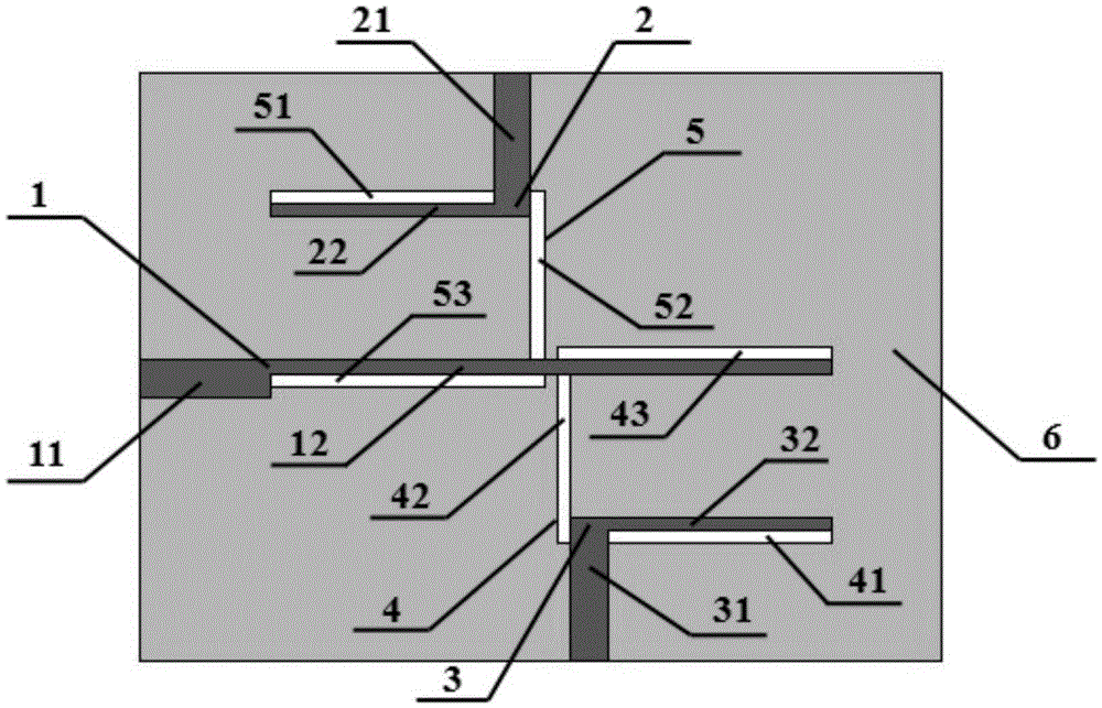
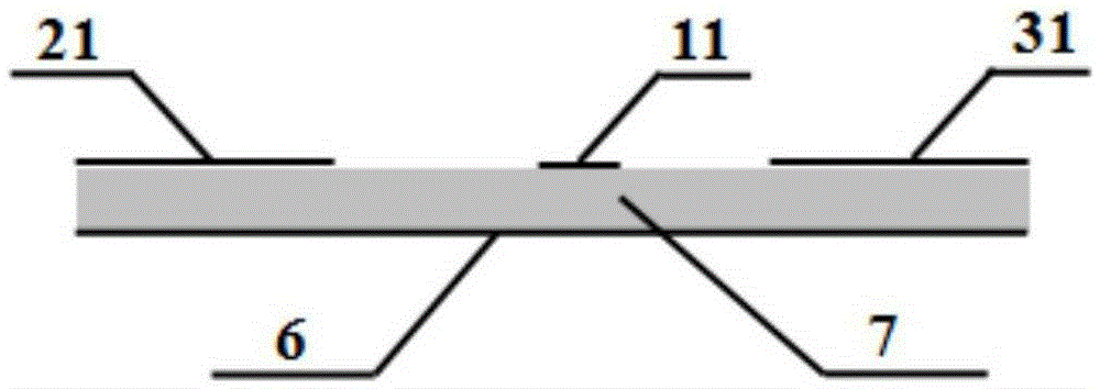
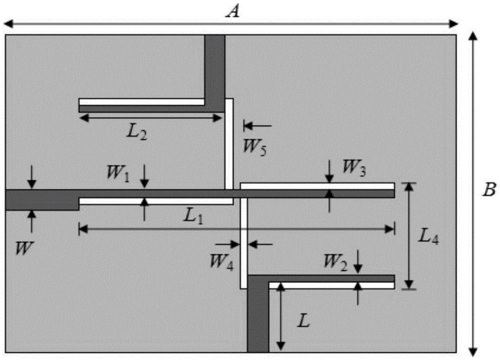
[0030] In this embodiment, the structural size of the broadband balun based on the microstrip line-slot line structure is as follows image 3 As shown, the size of the dielectric substrate 7 is A x B =24.3×22.8mm 2 , the width and length of the 50 ohm microstrip line conduction strip 11, 50 ohm microstrip line conduction strip 21 and 50 ohm microstrip line conduction strip 31 etched on the front side of the dielectric substrate 7 are W =1.18mm, L =4mm; the width and length of the half-wavelength transmission line 12 are W 1 =0.8mm, L 1 =16.6mm, the width and length of the first quarter-wavelength transmission line 22 and the second quarter-wavelength transmission line 32 are W 2 =0.3mm, L 2 =8mm; the width and length of the outer groove lines of the first U-shaped groove line 4 and the second U-shaped groove line 5 are W 3 =0.1mm, L 2 =8mm, the width and length of the groove line in the middle part are W 4 =0.2mm, L 3 =8mm, the distance between the groove lin...


PUM

PropertyMeasurementUnit
Bending angleaaaaaaaaaa
Thicknessaaaaaaaaaa

Abstract

The invention discloses a wideband balun based on a microstrip line-slot structure. The wideband balun comprises an input end microstrip line conduction band and two output end microstrip line conduction bands, which are arranged on the upper surface of a dielectric substrate, wherein two sections of U-shaped slot lines and a metal ground plate are arranged on the lower surface of the dielectric substrate; the input end microstrip line conduction band and the middle portions of the two sections of U-shaped slot lines form a vertical three-dimensional cross structure, and the input end microstrip line conduction band is parallel to internal slot lines; the two output end microstrip line conduction bands are respectively arranged on two sides of the input end microstrip line conduction band, extend from the edge of the dielectric substrate to the input end microstrip line conduction band and have tail ends folded to be L-shaped; the folded portions of the two output end microstrip line conduction bands are parallel to the external slot lines of the U-shaped slot lines, and the output end microstrip line conduction bands on the two sides are distributed in central symmetry about the midpoint of the input end microstrip line conduction band. The wideband balun has the advantages of compact structure, low insertion loss, good matching characteristic and the like, and facilitates broadband and miniaturization development of wireless communication.

Description

technical field [0001] The invention relates to the technical field of microwave passive devices, in particular to a broadband balun based on a novel interconnection structure. Background technique [0002] The balun is a balanced unbalanced converter, which can realize the equal-amplitude and anti-phase distribution of power and the function of impedance matching. Its application fields are very wide. For example, in the antenna field, for a differential antenna, a balun is needed to convert an unbalanced signal into a balanced signal to feed it. At present, the most common signal transmission line in microwave integrated circuits is microstrip line, which transmits unbalanced signals, while coplanar waveguide and coplanar stripline are single-sided transmission lines, which are small in size, easy to integrate, and easy to realize with microstrip structure. Features such as broadband interconnection structure. Based on this background, we use the microstrip line-slot lin...

Claims


Application Information

Patent Timeline
IPC IPC(8): H01P5/10
Inventor 马卉黄烽刘琳李昱燃王建朋
Owner NANJING UNIV OF SCI & TECH
Why Eureka
Try Eureka