A Method for Reducing Threshold Voltage Fluctuation of High-k Metal Gate Devices
A threshold voltage, metal gate technology, used in semiconductor devices, semiconductor/solid-state device manufacturing, circuits, etc., can solve problems such as threshold voltage drift and high leakage, and achieve the effect of reducing threshold voltage fluctuations and small work function fluctuations
- Summary
- Abstract
- Description
- Claims
- Application Information
AI Technical Summary
Problems solved by technology
Method used
Image
Examples
Embodiment 1
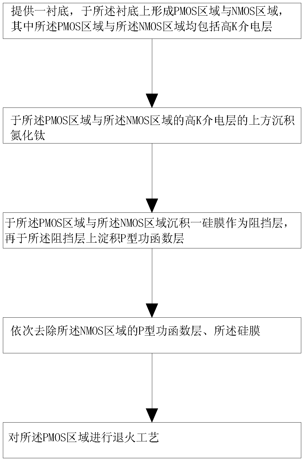
[0030] figure 1 It is a schematic diagram of a method for reducing threshold voltage fluctuations of high-K metal gate devices according to the present invention, such as figure 1 As shown, the method of this embodiment includes: providing a substrate, forming a PMOS region and an NMOS region on the substrate, wherein both the PMOS region and the NMOS region include a high-K dielectric layer; Deposit titanium nitride (TiN) on the top of the electrical layer; deposit a silicon film in the PMOS area and the NMOS area as a barrier layer, and then deposit a P-type work function layer on the barrier layer; remove the P-type work function layer in the NMOS area, Silicon film; perform an annealing process on the PMOS region.
Embodiment 2
[0032] Figure 2a-2f It is a process flow diagram of Embodiment 2 of a barrier layer that reduces threshold voltage fluctuations of high-K metal gate devices according to the present invention, as shown in Figure 2a As shown, a silicon substrate 100 is provided, a silicon nitride (SiN) layer is deposited on the substrate 100, a PMOS region and an NMOS region are formed inside the silicon nitride layer 102, and the PMOS region and the NMOS region are sequentially arranged from outside to inside. An intermediate layer 101 , a high-K dielectric layer 103 , and a titanium nitride layer 104 .
[0033] Such as Figure 2b As shown, a silicon film 105 is deposited on the titanium nitride layer 104 by atomic layer deposition equipment, and the silicon film 105 is used as a barrier layer, wherein the silicon film 105 is deposited on both the PMOS and NMOS regions. The thickness of the above-mentioned deposited silicon film 105 is
[0034] Such as Figure 2c As shown, a P-type wor...
PUM
 Abstract
Description
Claims
Application Information
 - R&D
- Intellectual Property
- Life Sciences
- Materials
- Tech Scout
- Unparalleled Data Quality
- Higher Quality Content
- 60% Fewer Hallucinations
Browse by: Latest US Patents, China's latest patents, Technical Efficacy Thesaurus, Application Domain, Technology Topic, Popular Technical Reports.
© 2025 PatSnap. All rights reserved.Legal|Privacy policy|Modern Slavery Act Transparency Statement|Sitemap|About US| Contact US: help@patsnap.com


