Seed crystal laying method and single crystal growth method through ingotting
A laying method and seed crystal technology, applied in the direction of single crystal growth, single crystal growth, crystal growth, etc., can solve the problems of prone to defect proliferation and reduce the minority carrier lifetime of silicon wafers, so as to inhibit the formation and proliferation of defects and reduce the defects. Producing the effect of sinking probability and large thermal stress
- Summary
- Abstract
- Description
- Claims
- Application Information
AI Technical Summary
Problems solved by technology
Method used
Image

Examples
Embodiment 1
[0021] A kind of laying method of seed crystal, is used for the casting of quasi-single crystal, is characterized in that, comprises the following steps:
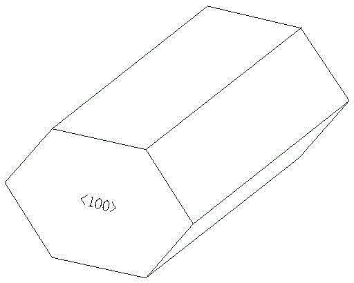
[0022] A: Make 36 pieces of regular hexagonal single crystal silicon seed crystals with a side length of 91mm. The normal direction of the section of the single crystal silicon columnar seed crystal is the crystal direction, and the thickness is 20mm; figure 1 As shown; there is no fixed requirement for the crystal orientation of the side normal direction of the single crystal silicon columnar seed crystal;
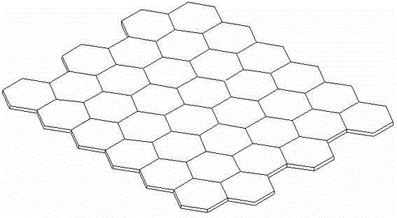
[0023] B: Spread 36 pieces of seed crystals on the bottom of the crucible in 6 rows×6 columns, and the sides of the seed crystals are closely matched; figure 2 shown.
Embodiment 2
[0025] A method for growing an ingot single crystal, characterized in that it comprises the steps of:
[0026] S1: Manufacture 36 regular hexagonal silicon single crystal seed crystals with a side length of 91 mm, the cross-sectional normal direction of the single crystal silicon columnar seed crystal is the crystal direction, and the thickness is 20 mm; figure 1 As shown; there is no fixed requirement for the crystal orientation of the side normal direction of the single crystal silicon columnar seed crystal;
[0027] S2: Spread 36 pieces of seed crystals on the bottom of the crucible in 6 rows×6 columns, and the sides of the seed crystals are closely matched; figure 2 shown;
[0028] S3: 700kg of silicon material is put into the crucible, and after melting, crystal growth, annealing and cooling, a quasi-monocrystalline silicon ingot is grown. During the melting step, the seed crystal with a thickness of about 5mm at the bottom is kept from being melted;
[0029] S4: Afte...
Embodiment 3
[0032] A method for growing an ingot single crystal, characterized in that it comprises the steps of:
[0033] S1: Manufacture 30 regular hexagonal silicon single crystal seed crystals with a side length of 112 mm, the cross-sectional normal direction of the single crystal silicon columnar seed crystal is the crystal direction, and the thickness is 20 mm; figure 1 shown;
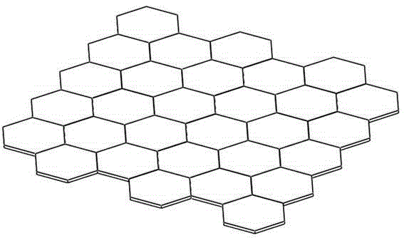
[0034] S2: Spread 30 seed crystals on the bottom of the crucible in 6 rows×5 columns, and the sides of the seed crystals are closely matched; image 3 shown;
[0035] S3: 920kg of silicon material is put into the crucible, and after melting, crystal growth, annealing and cooling, a quasi-single crystal silicon ingot is grown. During the melting step, the seed crystal with a thickness of about 3mm at the bottom is kept from being melted;
[0036] S4: After squaring the silicon ingot, cut it into quasi-monocrystalline silicon wafers with a side length of 156 mm and a thickness of 0.18 mm with a crystal orie...
PUM
| Property | Measurement | Unit |
|---|---|---|
| thickness | aaaaa | aaaaa |
| thickness | aaaaa | aaaaa |
Abstract
Description
Claims
Application Information
 - R&D
- Intellectual Property
- Life Sciences
- Materials
- Tech Scout
- Unparalleled Data Quality
- Higher Quality Content
- 60% Fewer Hallucinations
Browse by: Latest US Patents, China's latest patents, Technical Efficacy Thesaurus, Application Domain, Technology Topic, Popular Technical Reports.
© 2025 PatSnap. All rights reserved.Legal|Privacy policy|Modern Slavery Act Transparency Statement|Sitemap|About US| Contact US: help@patsnap.com