Semiconductor light-emitting device
A light-emitting device and semiconductor technology, which is applied in the direction of semiconductor devices, electrical components, circuits, etc., can solve the problems of limited use, single light-emitting center wavelength, etc.
- Summary
- Abstract
- Description
- Claims
- Application Information
AI Technical Summary
Problems solved by technology
Method used
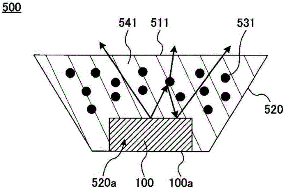
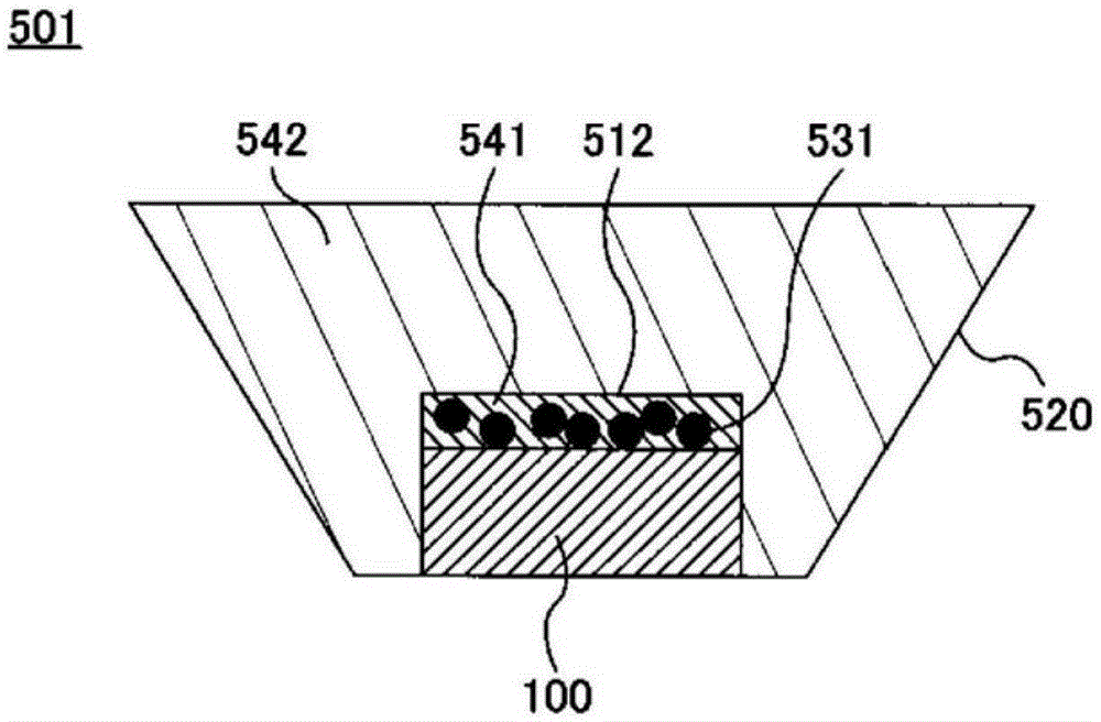
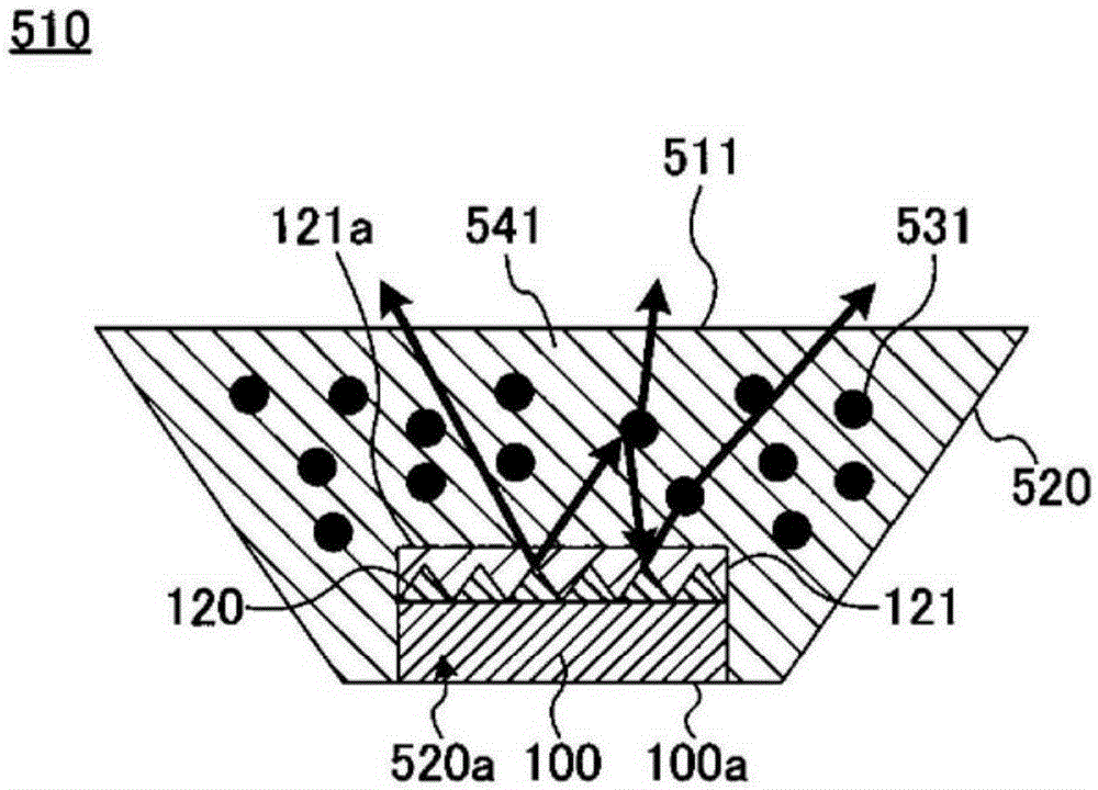
Image

Examples
Embodiment 1
[0313] (Making a cylindrical mold (Making a mold for making a resin mold))
[0314] As the base material for the semiconductor light emitting element of the cylindrical mold, a cylindrical quartz glass roll having a diameter of 80 mm and a length of 50 mm was used. On the surface of this cylindrical quartz glass roll, a fine structure (fine concavo-convex structure) was formed by the following method and using a direct drawing photolithography method using a semiconductor pulse laser.
[0315] First, a resist layer is formed by sputtering on the fine structure of the quartz glass surface. The sputtering method uses CuO as a target (anti-corrosion layer) and is implemented with RF100W power. The film thickness of the resist layer after film formation was 20 nm. The cylindrical mold produced as described above was rotated at a linear speed of s=1.0 m / sec, and exposure was performed under the following conditions to produce cylindrical molds having two types of long periods.
[0316]...
Embodiment 2
[0407] The cylindrical mold produced in the same manner as in Example 1 was exposed under the following conditions while rotating at a linear velocity of s=1.0 m / sec.
[0408] Cylindrical mold C
[0409] Wavelength of semiconductor laser for exposure: 405nm
[0410] Exposure laser power: 3.5mW
[0411] Px in the X-axis direction: 260nm
[0412] The variation range of the pitch Px with respect to the X-axis direction δ2: 26nm
[0413] The long period unit in the X-axis direction of the variation range δ2 PxL1: 2.60μm
[0414] Py in the Y-axis direction: 300nm
[0415] The variation range of the pitch Py with respect to the Y-axis direction δ1: 30nm
[0416] Long period unit in the Y-axis direction of the fluctuation range δ1 PyL1: 2.60μm
[0417] Long period unit in the Y-axis direction of the fluctuation range δ1 PyL2: 1.30μm
[0418] The pitch Py in the Y-axis direction is determined as follows. Based on the Z-phase signal of the spindle motor, the time T required for one cycle is measured,...
Embodiment 3
[0448] The same semiconductor light emitting element as in Example 2 was placed in the package and electrically connected to the electrode pad via Au wires. Then, the package is filled with a wavelength conversion member in which a fluorescent material having the following main wavelength is mixed with silicone resin.
[0449] 530nmβ-SiAlON: Eu
[0450] 580nmCa-α-SiAlON: Eu
[0451] 650nmCaAlSiN 3 : Eu
[0452] Table 4 shows the emission output ratio of Example 3 at 20 mA. In Example 3, similar to Example 1 and Example 2, light emission with glare peculiar to diffraction was not observed, and light emission angle dependence was hardly observed.
PUM
 Abstract
Description
Claims
Application Information
 - Generate Ideas
- Intellectual Property
- Life Sciences
- Materials
- Tech Scout
- Unparalleled Data Quality
- Higher Quality Content
- 60% Fewer Hallucinations
Browse by: Latest US Patents, China's latest patents, Technical Efficacy Thesaurus, Application Domain, Technology Topic, Popular Technical Reports.
© 2025 PatSnap. All rights reserved.Legal|Privacy policy|Modern Slavery Act Transparency Statement|Sitemap|About US| Contact US: help@patsnap.com