
A kind of multi-layer nanocomposite thin film material and preparation method thereof for high-density phase-change memory

A phase-change memory and nano-composite technology, applied in the field of multi-layer nano-composite thin film materials, can solve problems such as not disclosed, achieve high data retention temperature, increase storage density, and improve thermal stability

Active Publication Date: 2018-06-26
NINGBO UNIV
View PDF3 Cites 0 Cited by
  • Summary
  • Abstract
  • Description
  • Claims
  • Application Information

AI Technical Summary

Problems solved by technology

At present, there is no public information about the combination of GaSb and Sb at home and abroad. 4 Related research reports on multi-layer nanocomposite thin film materials and their preparation methods combined with Te for high-density phase-change memory

Method used


Image

  • A kind of multi-layer nanocomposite thin film material and preparation method thereof for high-density phase-change memory
  • A kind of multi-layer nanocomposite thin film material and preparation method thereof for high-density phase-change memory
  • A kind of multi-layer nanocomposite thin film material and preparation method thereof for high-density phase-change memory

Examples


Embodiment 1

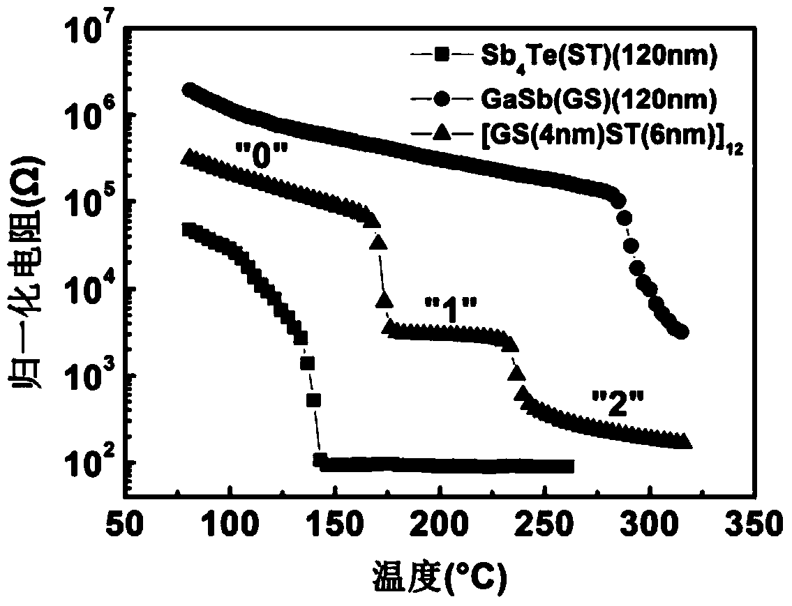
[0021] A kind of multilayer nanocomposite thin film material for high density phase change memory, the chemical structural formula of this multilayer nanocomposite thin film material is [GaSb / Sb 4 Te] x , where the thickness of the single-layer GaSb film is 4nm, and the single-layer Sb 4 The thickness of Te film is 6nm; x indicates single layer GaSb and single layer Sb 4 The number of alternating periods or layers of the Te thin film, x can be any integer between 1-15.

Embodiment 2

[0023] The steps of the preparation method of the multi-layer nanocomposite film material used in the above-mentioned embodiment 1 for high-density phase-change memory are as follows:

[0024] In the magnetron sputtering coating system, the cleaned quartz sheet or silicon oxide substrate is used to install the GaSb alloy target in the magnetron radio frequency sputtering target, and the Sb 4 The Te alloy target is installed in the DC sputtering target, and the sputtering chamber of the magnetron sputtering coating system is vacuumed until the vacuum degree in the chamber reaches 2.0×10 -4 Pa, then for GaSb alloy targets and Sb 4 The Te alloy target was pre-sputtered for 10 minutes, and the sputtering power of the GaSb alloy target was controlled to 20W, and the Sb 4 The sputtering power of Te alloy target is 15W, alternately sputtering GaSb film and Sb at room temperature 4 Te thin film until the total thickness of sputtering is 120nm, that is, GaSb / Sb 4 Te multilayer nanoc...

Embodiment 3

[0027] The specific steps of the preparation method of the multi-layer nanocomposite film material in the above-mentioned specific embodiment 2 are as follows:

[0028] 1. Clean SiO2 2 / Si(100) substrate, cleaning the surface and back, removing dust particles, organic and inorganic impurities

[0029] a) Strong ultrasonic cleaning in acetone solution for 3-5 minutes, rinse with deionized water;

[0030] b) Strong ultrasonic cleaning in ethanol solution for 3-5 minutes, rinse with deionized water, high-purity N 2 Blow dry the surface and back;

[0031] c) Dry the water vapor in an oven at 80°C for about 20 minutes;

[0032] 2. Preparation of GaSb / Sb by magnetron sputtering method 4 Preparation of Te multilayer composite film

[0033] a) Install GaSb and Sb 4 Te sputtering target, the purity of the target reaches 99.999% (atomic percentage), and the background vacuum is pumped to 2.0×10 -4 Pa;

[0034] b) Set the RF target sputtering power to 20W, and the DC target sputte...


PUM

PropertyMeasurementUnit
thicknessaaaaaaaaaa
thicknessaaaaaaaaaa
thicknessaaaaaaaaaa

Abstract

The invention discloses a multi-layer nano-composite film material for high-density phase-change memory and its preparation method, which is characterized in that the multi-layer nano-composite film material is a GaSb / Sb4Te multi-layer composite film, and its structure conforms to the following general formula: [ GaSb / Sb4Te]x, where the thickness of the single-layer GaSb thin film is 4nm, and the thickness of the single-layer Sb4Te thin film is 6nm, x represents the number of alternating periods or alternate layers of the single-layer GaSb and single-layer Sb4Te thin films, and the value is 1‑ Any integer between 15, the preparation method includes cleaning the substrate; installing the sputtering target; first sputtering the GaSb target, then sputtering the Sb4Te target, and then alternately sputtering the GaSb thin film and the Sb4Te thin film. Yes, the advantage is that it can realize multi-level storage, which greatly improves the storage density of the memory; it has a high ten-year data retention temperature, which can improve the thermal stability of the memory.

Description

technical field [0001] The invention relates to a material in the technical field of microelectronics, in particular to a multilayer nanocomposite thin film material used for high-density phase-change memory. Background technique [0002] In recent years, phase change memory (PCRAM) has attracted more and more researchers' attention, and is a hot spot in memory research at present, and is considered to be the most promising memory to become the mainstream of the next generation. The principle of phase change memory is to use the Joule heat generated by the storage medium under the action of electric pulses to make the storage medium convert between crystalline (low resistance) and amorphous (high resistance) states to realize information writing and erasing , The readout of information is realized by measuring the resistance value of the memory. PCRAM has the advantages of high storage density, low power consumption, fast reading speed, strong stability, and compatibility w...

Claims


Application Information

Patent Timeline
Patent Type & Authority Patents(China)
IPC IPC(8): H01L45/00H01L27/24B82Y30/00B82Y40/00
CPCB82Y30/00B82Y40/00H10B63/00H10N70/00
Inventor 吕业刚王苗沈祥王国祥戴世勋
Owner NINGBO UNIV
Learn More