

High-quality shielded diffusion method for heavily doped silicon substrates
A diffusion method and silicon substrate technology, which is applied in the manufacture of electrical components, circuits, semiconductors/solid-state devices, etc., can solve problems affecting the consistency of chip parameters and the consistency of junction depth in the chip, so as to improve market competitiveness and Cost-effective, improved consistency of chip parameters, and improved quality
- Summary
- Abstract
- Description
- Claims
- Application Information
AI Technical Summary
Problems solved by technology
Method used
Image

Examples
Embodiment Construction
[0021] The present invention will be described in further detail below in conjunction with the accompanying drawings.
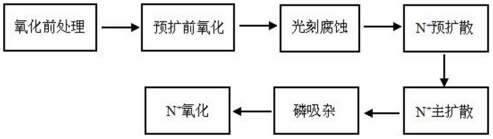
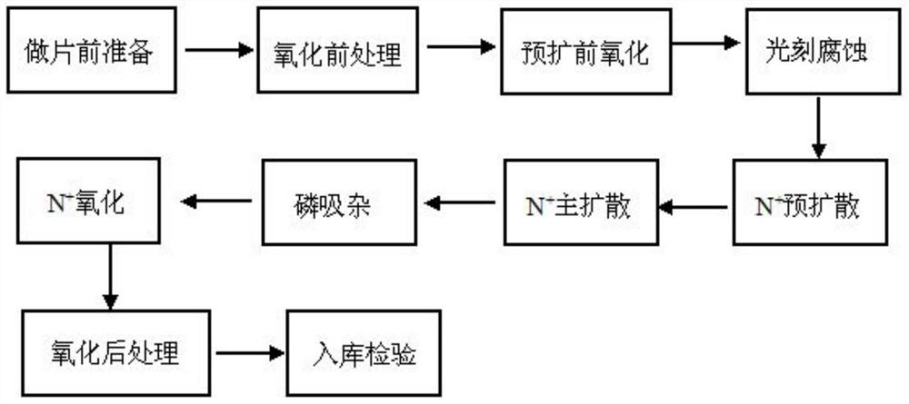
[0022] Such as figure 2 As shown, the process flow of the high-quality shielded diffusion method using heavily doped silicon substrates includes the following steps:
[0023] Step 1: Prepare before waving, inspect the electrical parameters, physical parameters and appearance of the silicon wafers, and carry out batch marking, and mark and distinguish the silicon wafers one by one according to the marking rules and the requirements of the accompanying work order;
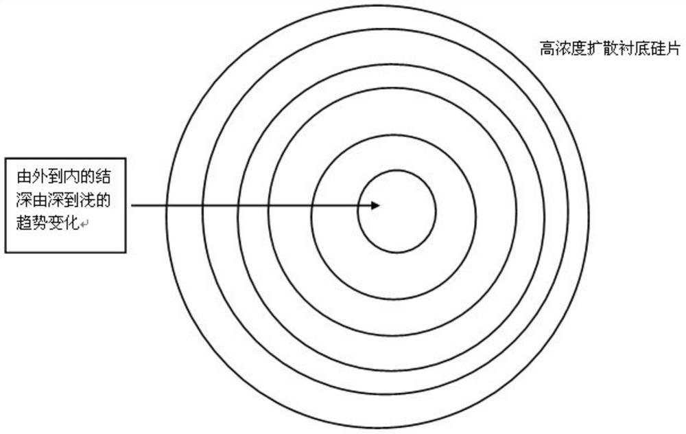
[0024] The second step: N+ pre-expansion pre-treatment, use acidic corrosive solution in FSI automatic cleaning machine and standard SC-1 / SC-2 / sulfuric acid cleaning solution to clean, to remove surface organic contamination and particle contamination before oxidation , Metal contamination and silicon single crystal damage purposes. Since the dry oxygen process currently used in oxidation has ver...
PUM
| Property | Measurement | Unit |
|---|---|---|
| thickness | aaaaa | aaaaa |
| thickness | aaaaa | aaaaa |
Abstract
Description
Claims
Application Information