
Manufacture method of TFT substrate

A manufacturing method and substrate technology, applied in semiconductor/solid-state device manufacturing, electrical components, electrical solid-state devices, etc., can solve the problems of high process cost, achieve the effects of simplifying the process, improving production efficiency, and saving production costs

Active Publication Date: 2016-03-09
TCL CHINA STAR OPTOELECTRONICS TECH CO LTD
View PDF4 Cites 6 Cited by
  • Summary
  • Abstract
  • Description
  • Claims
  • Application Information

AI Technical Summary

Problems solved by technology

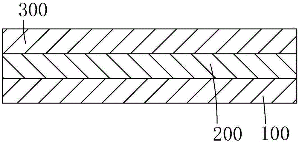
[0014] Step 8, such as Figure 8 As shown, an interlayer insulating layer 900, a source / drain 910, a flat layer 920, a cathode 930, and a pixel definition layer 940 are formed on the gate insulating layer 700 and the gate 800, and finally OLED950 is evaporated to complete The whole process of TFT substrate requires nine mask definitions before OLED evaporation can be performed, and the process cost is relatively high

Method used


Image

  • Manufacture method of TFT substrate
  • Manufacture method of TFT substrate
  • Manufacture method of TFT substrate

Examples


Embodiment Construction

[0055] In order to further illustrate the technical means adopted by the present invention and its effects, the following describes in detail in conjunction with preferred embodiments of the present invention and accompanying drawings.

[0056] see Figure 9 , the invention provides a kind of manufacturing method of TFT substrate, comprises the following steps:

[0057] Step 1, such as Figure 10 As shown, a substrate 1 is provided, a buffer layer 2 is deposited on the substrate 1 , and an amorphous silicon layer 3 is deposited on the buffer layer 2 .

[0058] Specifically, the substrate 1 is a glass substrate.

[0059] Specifically, the buffer layer 2 is a silicon nitride (SiNx) layer, a silicon oxide (SiOx) layer, or a composite layer of the two; the thickness of the buffer layer 2 is

[0060] Specifically, the thickness of the amorphous silicon layer 3 is

[0061] Step 2, such as Figure 11 As shown, the amorphous silicon layer 3 is ion-implanted and baked at a hig...


PUM


Abstract

The invention provides a manufacture method of a TFT substrate. After that ion implantation and induced crystallization are carried out on an amorphous silicon layer, it is not required to completely remove an ion induction layer at the surface of an obtained polysilicon layer, instead, only the ion induction layer in a channel region is removed in a half-toning photomask technology, it is not required to carry out ion implantation on a subsequent source / drain electrode contract area again, and a photomask needed by ion implantation again can be saved; source / drain electrodes are prepared under the half-toning photomask, so that a photomask needed by manufacture of the source / drain electrodes can be saved; and the source / drain electrodes are manufactured at first, manufacture of an interlayer insulation layer is omitted, and a photomask needed by manufacture of the interlayer insulation layer is further saved. According to the manufacture method of the TFT substrate, the half-toning photomask technology is used to reduce nine photomasks needed in the prior art to six photomasks, thereby effectively simplifying the process, improving the production efficiency and reducing the production cost.

Description

technical field [0001] The invention relates to the field of display technology, in particular to a method for manufacturing a TFT substrate. Background technique [0002] Thin Film Transistor (TFT for short) is the main driving element in the current Liquid Crystal Display (LCD for short) and Active Matrix Organic Light-Emitting Diode (AMOLED for short), and is directly related to high performance. The development direction of the flat panel display device. [0003] Low Temperature Poly-silicon (LTPS) technology is a new generation of TFT substrate manufacturing technology. The biggest difference from traditional amorphous silicon (a-Si) technology is that low-temperature poly-silicon displays have a faster response speed and have high brightness and high resolution. advantages of high speed and low power consumption. [0004] At present, the LTPS crystallization process includes excimer laser annealing (Excimer Laser Anneal, ELA) technology and solid phase crystallizatio...

Claims


Application Information

Patent Timeline
IPC IPC(8): H01L21/77
CPCH01L21/77H01L27/1288H01L29/66757H01L29/78675H01L27/1277H01L21/02532H01L27/124H01L29/66765H10K71/00H10K50/82H10K59/122H10K59/123H10K59/124H01L27/1274H01L29/495H01L29/513H01L29/518
Inventor 张晓星
Owner TCL CHINA STAR OPTOELECTRONICS TECH CO LTD
Learn More