Novel organic electroluminescent compounds and organic electroluminescent device comprising the same

A compound and luminescent technology, applied in organic chemistry, luminescent materials, chemical instruments and methods, etc., can solve the problems of high driving voltage, decomposition, low glass transition temperature, etc., achieve high electron transmission efficiency, reduce voltage requirements, Effect of Improving Current Characteristics

Active Publication Date: 2016-03-09
ROHM & HAAS ELECTRONIC MATERIALS LLC
View PDF4 Cites 11 Cited by
  • Summary
  • Abstract
  • Description
  • Claims
  • Application Information

AI Technical Summary

Problems solved by technology

[0005] Although these phosphorescent host materials provide good emission characteristics, they have the following disadvantages: (1) Due to their low glass transition temperature and poor thermal stability, they may decompose in vacuum during high temperature deposition process
Therefore, organic EL devices using conventional phosphorescent materials have no advantage in power efficiency (lm / W)
(3) In addition, the operating life and luminous efficiency of organic EL devices are unsatisfactory
However, an organic EL device comprising the compound has a high driving voltage and contains a hole blocking layer, thereby increasing the voltage requirement of the device

Method used


Image

  • Novel organic electroluminescent compounds and organic electroluminescent device comprising the same
  • Novel organic electroluminescent compounds and organic electroluminescent device comprising the same
  • Novel organic electroluminescent compounds and organic electroluminescent device comprising the same

Examples


example 1

[0097] Example 1: Preparation of compound H-2

[0098]

[0099] Preparation of compound H-2-2

[0100] Compound H-2-1 (60.0 g, 263.0 mmol), 2-bromonitrobenzene (44.2 g, 219.0 mmol), tetrakis(triphenylphosphine)palladium(0) were stirred at reflux in a 2L round bottom flask (RBF). [Pd(PPh 3 ) 4 ] (7.6g, 6.57mmol), K 2 CO 3 (60.5g, 438.0mmol), toluene (900.0mL), ethanol (EtOH) (220.0mL) and H 2 O (220.0 mL). After 5 h, the mixture was washed with dichloromethane (DCM) and H 2 O extraction, and DCM layer in MgSO 4 Dry and filter. The resulting solid was dissolved in CHCl 3 and separated by silica gel column chromatography to obtain compound H-2-2 (74.8 g, 93%).

[0101] Preparation of compound H-2-3

[0102] Compound H-2-2 (74.8g, 245.0mmol), triethyl phosphite [P(OEt) 3 ] (500.0 mL) and 1,2-dichlorobenzene (1,2-DCB) (200.0 mL). After 13 hours, the solvent was distilled off and the solid was dissolved in CHCl 3 and separated by silica gel column chromatograph...

example 2

[0119] Device Example 2: Fabrication of OLED Devices Using Organic Electroluminescent Compounds of the Invention

[0120] An OLED device was fabricated in the same manner as in Device Example 1, except that Compound H-2 as a host was introduced into one unit of a vacuum vapor deposition apparatus, Compound D-88 as a dopant was introduced into the other unit, and both The materials were evaporated at different rates and the dopant was deposited at a doping amount of 4% by weight based on the total weight of the host and the dopant, forming a light-emitting layer with a thickness of 30 nm on the hole transport layer. Next, 2-(4-(9,10-bis(naphthalene-2-yl)anthracen-2-yl)phenyl)1-phenyl-1H-benzo[d]imidazole was introduced into one unit, and Lithium quinolate was introduced in one unit, and the two materials were evaporated at the same rate and deposited at a doping amount of 50% by weight, respectively, to form an electron transport layer with a thickness of 30 nm on the light e...


PUM

PropertyMeasurementUnit
Thicknessaaaaaaaaaa
Thicknessaaaaaaaaaa

Abstract

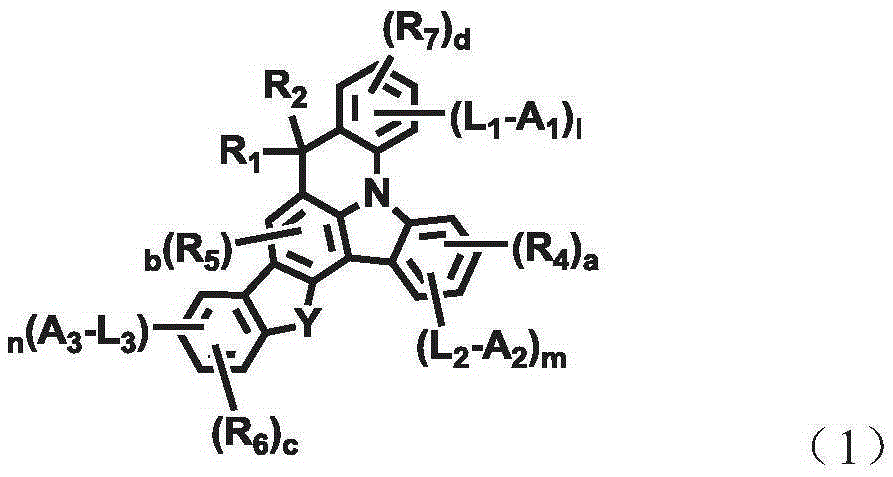
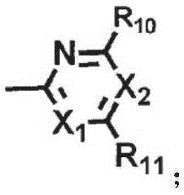
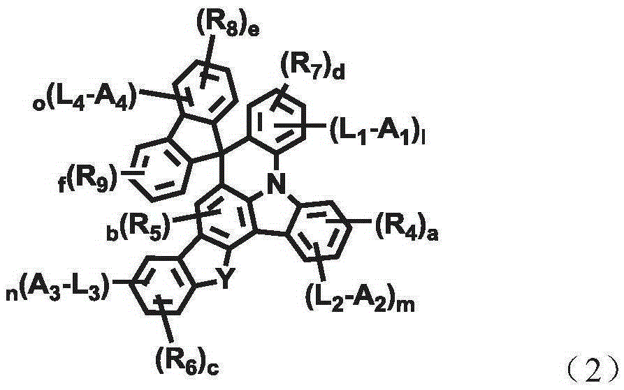
The present invention relates to a novel organic electroluminescent compound and an organic electroluminescent device comprising the same. The organic electroluminescent compound according to the present invention has high electron transport efficiency, which can prevent crystallization during the formation of the device; is effective in forming a layer(s) to improve the current property of the device, and thus reduces the driving voltage of the device; and has the advantages of providing an OLED device having advanced power efficiency. While organic electroluminescent devices comprising conventional organic electroluminescent compounds need hole blocking layers, the organic electroluminescent device comprising the organic electroluminescent compound of the present invention does not have to comprise a hole blocking layer, and thus can decrease the voltage needs of the device.

Description

technical field [0001] The present invention relates to novel organic electroluminescent compounds and organic electroluminescent devices containing said compounds. Background technique [0002] Electroluminescent (EL) devices are self-luminous devices, which have the advantage of offering wider, higher contrast ratios, and faster response times. The organic EL device was originally developed by Eastman Kodak by using small aromatic diamine molecules and aluminum complexes as materials for forming the light emitting layer [see Appl. Phys. Lett. 51, 913, 1987]. [0003] The most important factor determining the luminous efficiency of an organic EL device is the luminescent material. Fluorescent materials have been widely used as light-emitting materials so far. However, in view of the mechanism of electroluminescence, it is one of the best approaches in theory to develop phosphorescent materials, which can increase the luminous efficiency by up to four (4) times compared t...

Claims


Application Information

Patent Timeline
IPC IPC(8): C07D495/16C07D491/16C09K11/06C07D487/16H01L51/54H01L27/32
CPCC07D491/16C07D495/16C07D471/16C09K11/06H10K85/654H10K85/657H10K85/342H10K50/11H10K2101/10C07D403/14H10K85/649H10K85/6574H10K85/6572
Inventor Y-K·金N-K·金C-S·金Y-J·曹K-J·李
Owner ROHM & HAAS ELECTRONIC MATERIALS LLC
Why Eureka
Try Eureka