Image sensor and manufacturing method thereof

A graphic sensor and manufacturing method technology, applied in the direction of electric solid-state devices, semiconductor devices, radiation control devices, etc., can solve the problems of reducing the performance of image sensors, reducing the fill factor of silicon photodiodes, and reducing device performance, etc.

Active Publication Date: 2016-03-23
SHANGHAI INTEGRATED CIRCUIT RES & DEV CENT
View PDF4 Cites 22 Cited by
  • Summary
  • Abstract
  • Description
  • Claims
  • Application Information

AI Technical Summary

Problems solved by technology

[0004] However, in recent years, as the pixel size of solid-state image sensors has become smaller and smaller, its light absorption area has also decreased. Due to the existence of active readout circuits, the fill factor of silicon photodiodes has continued to decrease, and the signal-to-noise ratio of the device has deteriorated.
In addition, due to the influence of the metal interconnection, only part of the incident light can enter the photodiode area, further degrading the performance of the image sensor
[0005] At the same time, the CMOS image sensor ...

Method used


Image

  • Image sensor and manufacturing method thereof
  • Image sensor and manufacturing method thereof
  • Image sensor and manufacturing method thereof

Examples


Embodiment 1

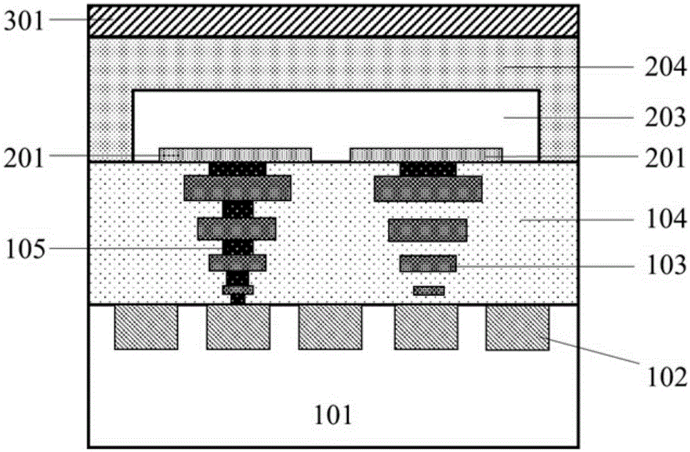
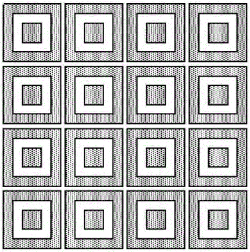
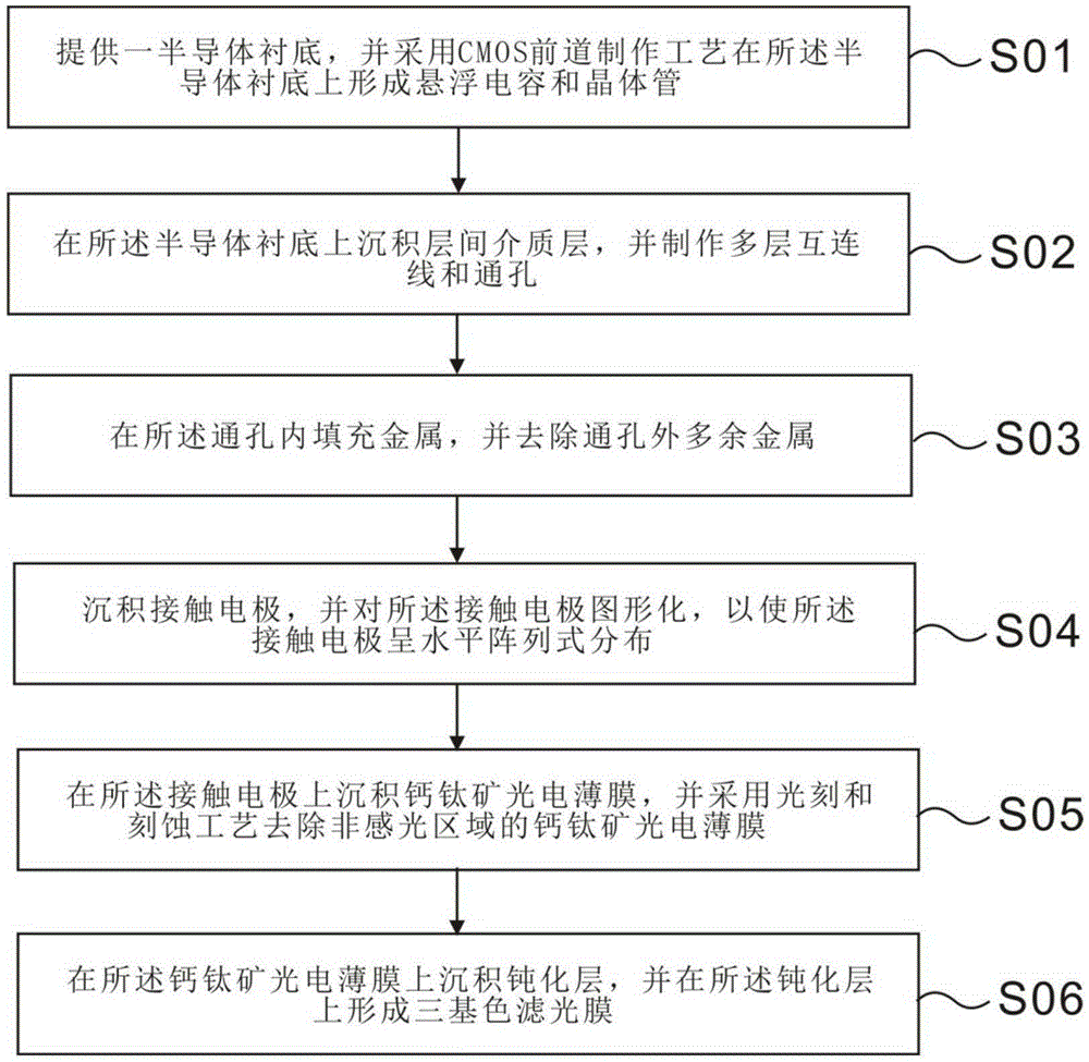
[0061] Such as figure 1 As shown, the present invention provides a kind of pattern sensor, and it comprises semiconductor substrate 101, interlayer dielectric layer 104, interconnection line 103, through hole 105, contact electrode 201, perovskite photoelectric thin film 203, passivation layer 204 and Three-color filter film 301, wherein the semiconductor substrate 101 has floating capacitors and transistors 102, the interlayer dielectric layer 104 is arranged on the upper surface of the semiconductor substrate 101, and the interlayer dielectric layer 104 has multi-layer interconnection lines 103 and 105 vias filled with metal, see figure 2 , the contact electrodes 201 are distributed in an array in the horizontal direction on the interlayer dielectric layer 104, and there is a preset width between adjacent contact electrodes, and the perovskite photoelectric thin film 203 covers the contact electrodes 201 to form In the photosensitive area of ​​the image sensor, the passiva...

Embodiment 2

[0078] Such as Figure 4 As shown, the present invention provides a kind of image sensor, and it comprises semiconductor substrate 101, interlayer dielectric layer 104, multilayer interconnection line 103, first through hole 105, contact electrode 201, perovskite photoelectric thin film 203, medium Thin film layer 205, top electrode 202, passivation layer 204, and three primary color filter films 301; wherein, there are floating capacitors and transistors 102 on the semiconductor substrate 101, and the interlayer dielectric layer 104 is arranged on the upper surface of the semiconductor substrate 101, and The interlayer dielectric layer 104 has a multilayer interconnection line 103 and a first through hole 105 filled with metal, please refer to Figure 5 , the contact electrodes 201 are distributed in an array in the vertical direction on the interlayer dielectric layer, and there is a preset width between adjacent contact electrodes 201; the perovskite photoelectric thin film...


PUM


Abstract

The invention belongs to the technical field of semiconductor integrated circuit manufacturing technology, and discloses an image sensor and a manufacturing method thereof. The image sensor comprises a semiconductor substrate, an interlayer dielectric layer, contact electrodes, a perovskite photoelectric film, a passivation layer and a three-primary-color filtering film. A photoelectric conversion unit is enabled to be separated from other functional units through introduction of the perovskite photoelectric film, and the two-dimensional planer structure of a conventional CMOS image sensor is optimized into a three-dimensional laminated structure. The image sensor based on the perovskite photoelectric film can have 100% of filling coefficient, and the chip size is greatly reduced. Besides, the technological requirement for extremely low noise of a silicon photodiode does not need to be considered in the manufacturing process of the chip so that the technological requirement can be reduced and cost can be substantially reduced.

Description

technical field [0001] The invention belongs to the technical field of semiconductor integrated circuit manufacturing technology, and relates to a pattern sensor and a manufacturing method thereof. Background technique [0002] Image sensors are an important part of digital cameras. According to different components, it can be divided into two categories: CCD (ChargeCoupledDevice, charge-coupled device) and CMOS (ComplementaryMetal-OxideSemiconductor, metal-oxide-semiconductor element). [0003] Pixel sensitivity, one of the important performance indicators of CMOS image sensors, is mainly determined by the product of the fill factor (the ratio of the photosensitive area to the entire pixel area) and the quantum efficiency (the number of electrons generated by photons bombarding the screen). In CMOS image sensors, active pixels are used in CMOS image sensors in order to achieve a noise index and sensitivity levels comparable to those of CCD converters. At the same time, th...

Claims


Application Information

Patent Timeline
IPC IPC(8): H01L27/146
CPCH01L27/14601H01L27/14665H01L27/14683
Inventor 耿阳胡少坚陈寿面
Owner SHANGHAI INTEGRATED CIRCUIT RES & DEV CENT
Why Eureka
Try Eureka