Manufacturing method for ultraviolet LED device

A technology for LED devices and manufacturing methods, applied in semiconductor devices, electrical components, circuits, etc., can solve the problems of difficult airtight packaging, temperature limitation of welding process, affecting the performance and reliability of LED devices, etc., so as to improve airtightness, The effect of prolonging the service life

Inactive Publication Date: 2016-03-23
FOSHAN CITY NANHAI DISTRICT LIANHE GUANGODNG XINGUANGYUAN IND INNOVATION CENT
View PDF4 Cites 10 Cited by
  • Summary
  • Abstract
  • Description
  • Claims
  • Application Information

AI Technical Summary

Problems solved by technology

Since the LED chip has completed the solid crystal and wire bonding process before welding, the temperature of the welding process is greatly limited (the temperature of the LED chip is lower than 260

Method used


Image

  • Manufacturing method for ultraviolet LED device
  • Manufacturing method for ultraviolet LED device
  • Manufacturing method for ultraviolet LED device

Examples


Embodiment approach 1

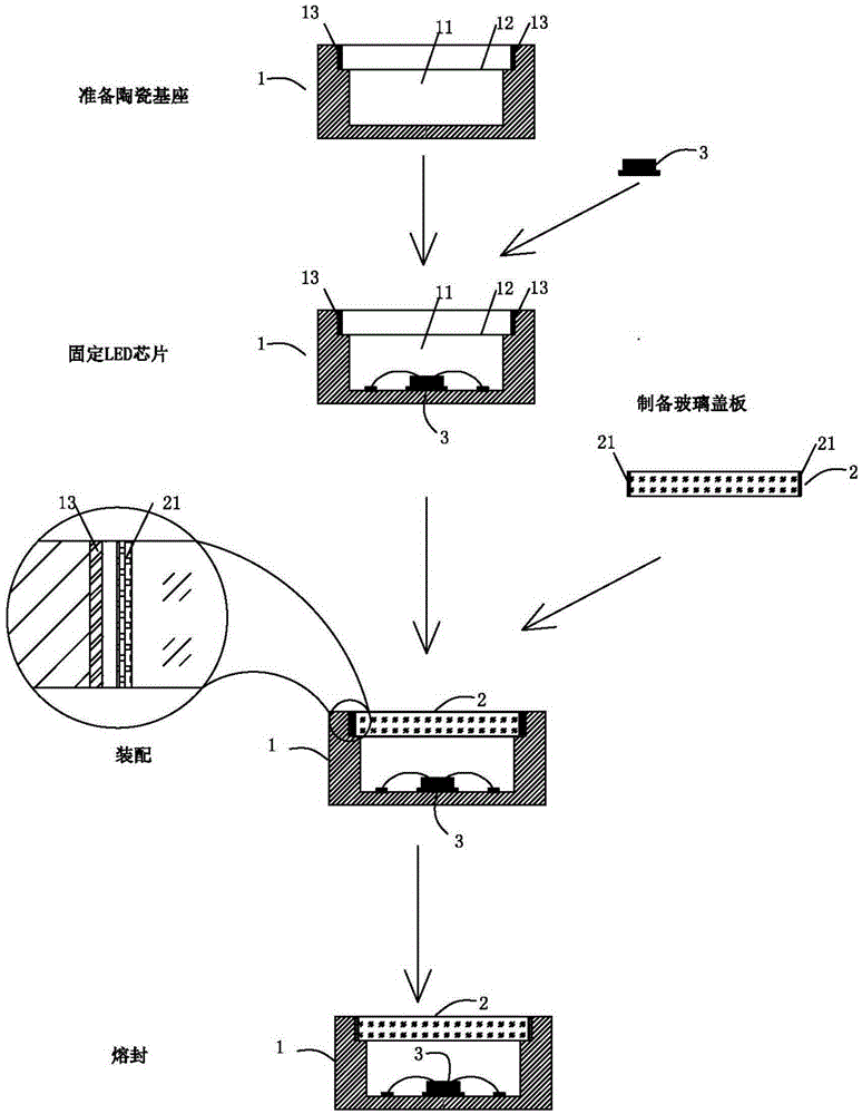
[0028] refer to figure 1 , a kind of manufacture method of ultraviolet LED device, comprises the following steps:

[0029] Prepare the ceramic base 1: the ceramic base 1 has a cavity 11, a groove 12 is arranged on the upper part of the cavity 11, and a metal layer 13 is formed on the side wall of the groove 12 by sputtering, evaporation or co-firing. The first metal layer 13 can be a copper film layer, a tin film layer or a silver film layer. The copper film layer, tin film layer and silver film layer mentioned here do not include the metal layer formed only by copper, tin or silver, but also include the film layer formed by the alloy mainly composed of copper, tin and silver. Preferably, the thickness of the first metal layer 13 is 10-30 μm, such as 10 μm, 20 μm, 25 μm, 30 μm and so on.

[0030] Fixing the LED chip 3: fixing the ultraviolet LED chip 3 on the bottom of the cavity 11 of the ceramic base 1 through crystal bonding and wire bonding processes.

[0031] Prepare t...

Embodiment approach 2

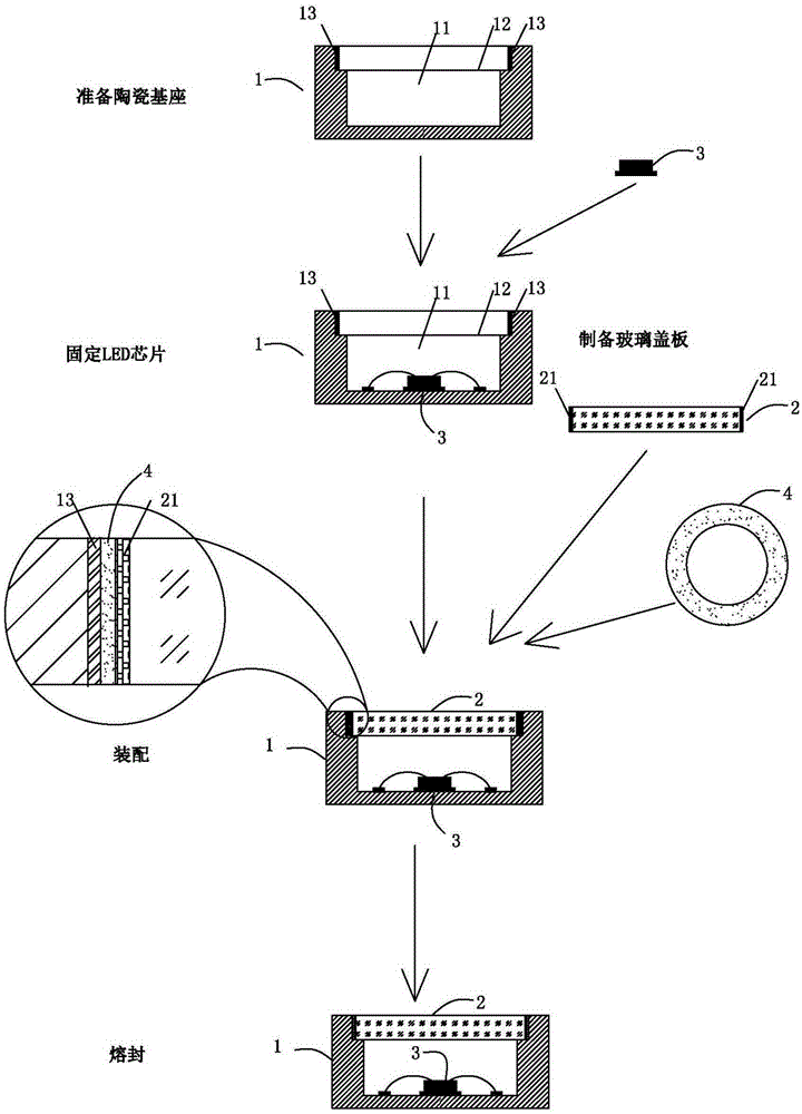
[0035] Or, as an improvement, in order to better realize fusion sealing, the manufacturing method of the present invention can refer to such as figure 2 The flowchart shown.

[0036] Prepare the ceramic base 1: the ceramic base 1 has a cavity 11, the upper part of the cavity 11 is provided with a groove 12, and the side wall of the groove 12 is provided with a metal layer 13 by sputtering, evaporation or co-firing; the metal layer 1 13 may be a copper film layer, a tin film layer or a silver film layer. The copper film layer, tin film layer and silver film layer mentioned here do not include the metal layer formed only by copper, tin or silver, but also include the film layer formed by the alloy mainly composed of copper, tin and silver. Preferably, the thickness of the first metal layer 13 is 10-30 μm, such as 10 μm, 20 μm, 25 μm, 30 μm and so on.

[0037] Fixing the LED chip 3: fixing the ultraviolet LED chip 3 on the bottom of the cavity 11 of the ceramic base 1 through ...


PUM

PropertyMeasurementUnit
Thicknessaaaaaaaaaa
Thicknessaaaaaaaaaa

Abstract

The invention discloses a manufacturing method for an ultraviolet LED device. The method comprises the steps of preparation of a ceramic substrate and a glass cover plate, assembling, melt sealing and the like. A metal layer is arranged at the joint of the ceramic substrate and the glass cover plate and then is molten in an electromagnetic induction heating or laser heating mode, thereby realizing low-temperature melt sealing of the metal layer, obtaining the fully inorganically packaged ultrasonic LED device, improving the airtightness, corrosion resistance and ultraviolet resistance of the device, and prolonging the service life of the device.

Description

technical field [0001] The invention belongs to LED packaging technology, and in particular relates to a method for manufacturing an ultraviolet LED device. Background technique [0002] For high-power LED packaging, in order to protect the LED chip, reduce the total reflection of the interface, and improve the light output efficiency of the LED, a layer of packaging glue (epoxy resin or silica gel) with a high refractive index is usually coated on the surface of the LED chip. In addition, in order to obtain white LEDs, phosphor powder is generally mixed with encapsulation glue, and then coated on blue LED chips. However, for the packaging of ultraviolet LED chips, the packaging glue is easily aged by ultraviolet radiation, which reduces the luminous efficiency and affects the performance and reliability of LED devices. Therefore, for the packaging of ultraviolet LEDs (especially the packaging of deep ultraviolet LEDs with a wavelength of less than 300nm), an adhesive-free ...

Claims


Application Information

Patent Timeline
IPC IPC(8): H01L33/00H01L33/48
CPCH01L33/483H01L2933/0033
Inventor 贺珂张亚菲宋定洁
Owner FOSHAN CITY NANHAI DISTRICT LIANHE GUANGODNG XINGUANGYUAN IND INNOVATION CENT
Why Eureka
Try Eureka