Multi-grating structure-based semiconductor laser beam combination device and beam combination method

A grating structure and laser technology, which is applied to semiconductor laser devices, semiconductor lasers, laser devices, etc., can solve the problems of poor quality of semiconductor laser beam combining beams, and achieve a simple and not cumbersome structure, simple installation and adjustment, and high structural stability. Effect

Inactive Publication Date: 2016-03-23
CHANGCHUN INST OF OPTICS FINE MECHANICS & PHYSICS CHINESE ACAD OF SCI
View PDF5 Cites 27 Cited by
  • Summary
  • Abstract
  • Description
  • Claims
  • Application Information

AI Technical Summary

Problems solved by technology

[0005] In order to solve the problem of poor quality of semiconductor laser beam combining existing in existing beam combining devices and beam combi

Method used


Image

  • Multi-grating structure-based semiconductor laser beam combination device and beam combination method

Examples


Embodiment Construction

[0034] The present invention will be described in further detail below in conjunction with the accompanying drawings.

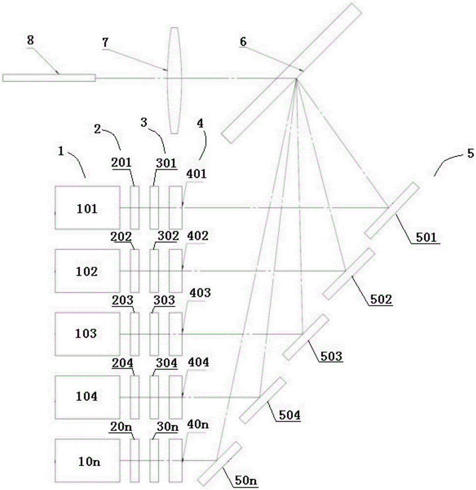
[0035] Such as figure 1 As shown, the semiconductor laser beam combining device based on the multi-grating structure of the present invention mainly includes a semiconductor laser group 1, a fast axis collimator mirror group 2, a slow axis collimator mirror group 3, a volume Bragg grating group 4, and a mirror group 5 , Diffraction grating 6, focusing mirror 7 and multimode fiber 8.

[0036] The semiconductor laser group 1 is composed of n semiconductor lasers 101-10n, the fast-axis collimating mirror group 2 is composed of n fast-axis collimating mirrors 201-20n, and the slow-axis collimating mirror group 3 is composed of n slow-axis collimating mirrors 301 ~30n, volume Bragg grating group 4 is composed of n individual Bragg gratings 401~40n, mirror group 5 is composed of n mirrors 501~50n, n is a positive integer and 2≤n≤1000.

[0037] Fast axis collimato...


PUM

PropertyMeasurementUnit
Thicknessaaaaaaaaaa
Reflection bandwidthaaaaaaaaaa
Focal lengthaaaaaaaaaa

Abstract

The invention discloses a multi-grating structure-based semiconductor laser beam combination device and beam combination method, relates to the field of semiconductor lasers and aims at solving the problem that existing device and method are poor in quality of semiconductor laser-combined beams. A semiconductor laser group in the device sends out combined beams which are the same in outgoing direction; the combined beams enter a volume Bragg grating group after the actions of a fast-axis collimating lens group and a slow-axis collimating lens group; one part of beams are reflected to corresponding semiconductor lasers to achieve locking of output wavelengths of the semiconductor laser group; the other part of beams enter corresponding reflectors, enter diffraction gratings for overlapping at different incident angles after being reflected through a reflector group, and are diffracted at the same diffraction angle; and outgoing beams of the semiconductor laser group are combined into one beam for outputting, and are coupled to a multi-mode optical fiber through a focus lens. A feedback resonant cavity is short in length; the structural stability is relatively high; assembly and adjustment are simple; and output powers of the semiconductor lasers are greatly improved under the premise of keeping relatively good beam quality.

Description

technical field [0001] The invention relates to the technical field of semiconductor lasers, in particular to a semiconductor laser beam combining device and a beam combining method based on a multi-grating structure. Background technique [0002] Semiconductor lasers have the advantages of small size, light weight, and high efficiency. They have been widely used in laser medical treatment, fiber laser pumping, laser cladding, and laser welding. However, the unit power of the semiconductor laser is small (less than 10 watts), the beam quality is poor (the fast axis is 30 degrees, the slow axis is 10 degrees), and the power density is low (kW / cm2). Watt-level direct light sources are used in laser processing, national defense and other fields. [0003] The existing geometrical optics beam combining method is to combine the space, polarization and wavelength of semiconductor lasers to achieve high power output. The beams emitted by multiple semiconductor lasers are combined ...

Claims


Application Information

Patent Timeline
IPC IPC(8): H01S5/06H01S5/40
CPCH01S5/06H01S5/4012
Inventor 彭航宇张俊付喜宏曹军胜王彪王立军
Owner CHANGCHUN INST OF OPTICS FINE MECHANICS & PHYSICS CHINESE ACAD OF SCI
Why Eureka
Try Eureka