

Fan-out package method of embedded silicon substrate
A packaging method and a fan-out technology, which is applied in the manufacture of electrical components, electrical solid devices, semiconductor/solid devices, etc., can solve the problems of poor chip-to-panel bonding accuracy, chip position movement, and difficult alignment, etc., to achieve Effects of increasing operability and precision, improving package quality and efficiency, and reducing package cost
- Summary
- Abstract
- Description
- Claims
- Application Information
AI Technical Summary
Problems solved by technology
Method used
Image

Examples
Embodiment 1
[0042] A fan-out packaging method embedded in a silicon substrate, comprising the steps of:
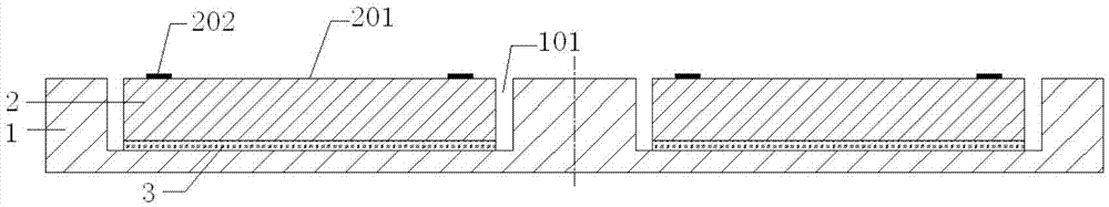
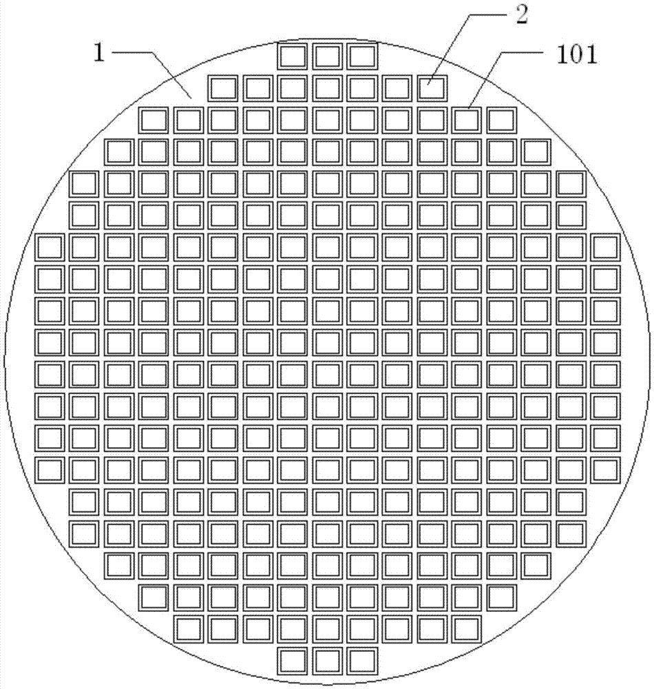
[0043] Step 1. See figure 1 , provide a silicon substrate wafer 1 with several grooves 101 made on the upper surface, at least one chip 2 is bonded in the groove, and the depth of the groove is equivalent to the thickness of the chip, and the soldering of the chip The disk surface 201 faces outward, that is, the bonding pad of the chip is close to the upper surface of the silicon base wafer. In order to facilitate the placement of the chip, the groove is slightly larger than the size of the chip, and glue or film needs to be used to fill the gap between the chip and the groove to increase the stability of the chip and ensure the insulation performance.
[0044] Preferably, the chip is bonded to the groove by glue or dry film 3 . More preferably, the glue or dry film is a non-conductive polymer glue or film, which bonds the chip and the bottom of the groove to ensure that the positio...
Embodiment 2
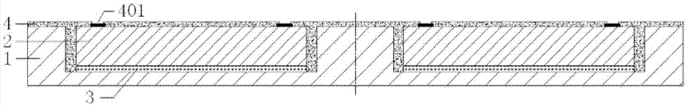
[0066] Such as figure 2 As shown, this embodiment 2 includes all the technical features of embodiment 1, the difference is that two chips 2 are embedded in a groove on the upper surface of the silicon substrate wafer, and the size and function of the two chips can be the same or the same. different. This embodiment can achieve the purpose of expanding the functions of the package.
[0067] To sum up, the present invention provides a fan-out packaging method embedded in a silicon substrate. First, the chip is mounted using the fan-out wafer-level packaging technology, that is, the chip is embedded on the silicon substrate wafer for packaging, and then the fan-out During the production process, a number of silicon substrate wafers that have completed chip mounting are pasted on a panel for overall operation. Finally, the silicon substrate wafers are peeled off from the panel for bump preparation or solder ball planting, and silicon substrate is cut. Wafer, forming a fan-out p...
PUM
 Abstract
Description
Claims
Application Information