

Low-resistivity P type gallium nitride material and preparation method thereof
A low-resistivity, gallium nitride technology, used in circuits, electrical components, semiconductor/solid-state device manufacturing, etc., to reduce the effect of acceptor compensation, reduce resistivity, reduce series resistance and turn-on voltage
- Summary
- Abstract
- Description
- Claims
- Application Information
AI Technical Summary
Problems solved by technology
Method used
Image

Examples
Embodiment Construction
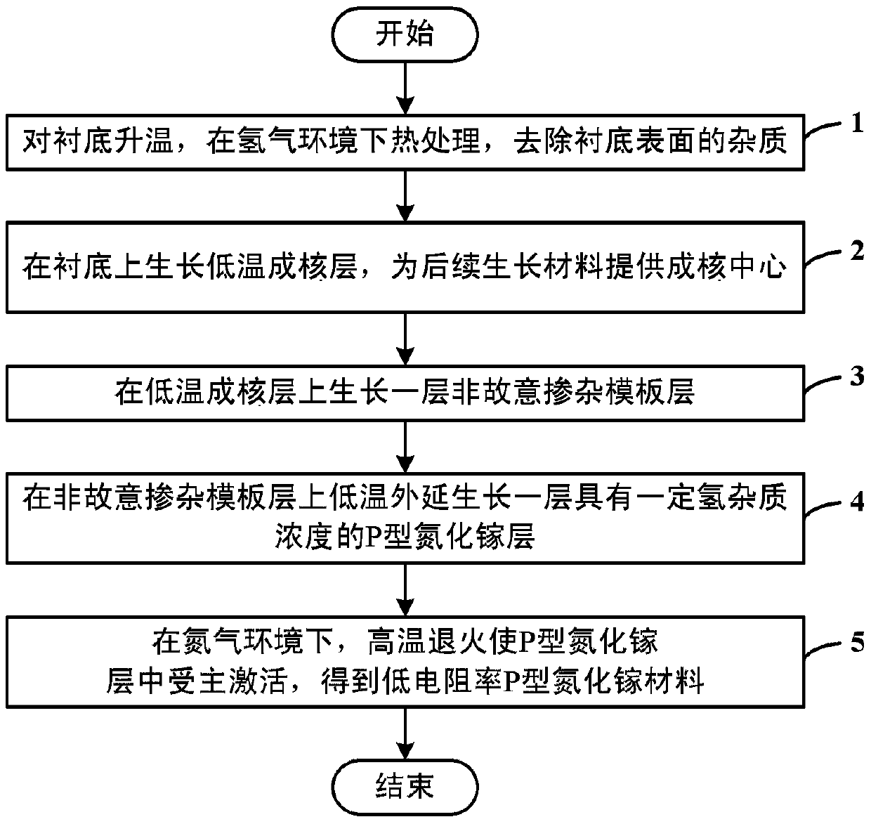
[0015] In order to make the object, technical solution and advantages of the present invention clearer, the present invention will be described in further detail below in conjunction with specific embodiments and with reference to the accompanying drawings.
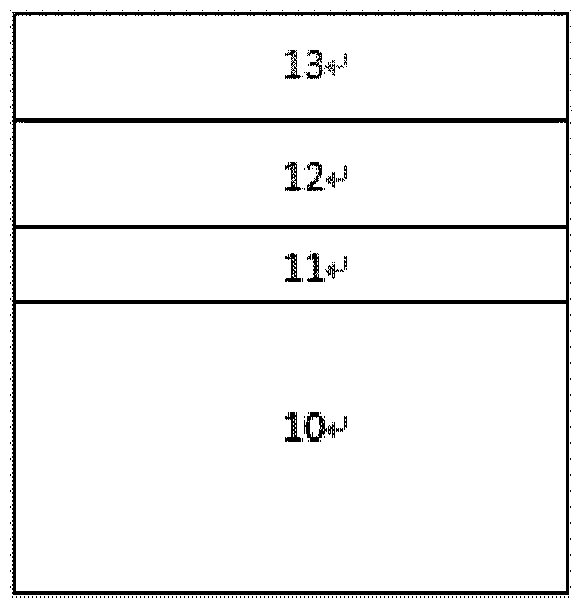
[0016] figure 1 A schematic structural view of a low-resistivity P-type gallium nitride material proposed by the present invention is shown. Such as figure 1 As shown, the low-resistivity P-type GaN material sequentially includes a substrate 10, a low-temperature nucleation layer 11, an unintentionally doped template layer 12, and a low-temperature grown P-type GaN with a certain hydrogen impurity concentration from bottom to top. Layer 13. Wherein: the substrate 10 is a sapphire substrate or a silicon carbide substrate or a gallium nitride substrate. The low-temperature nucleation layer 11 is fabricated on the substrate 10, its material is gallium nitride or aluminum nitride, the growth temperature is 500-600°C, and t...
PUM
| Property | Measurement | Unit |
|---|---|---|
| thickness | aaaaa | aaaaa |
| temperature | aaaaa | aaaaa |
Abstract
Description
Claims
Application Information