

Imaging spectrometer on the basis of etched diffraction grating
An imaging spectrometer and diffraction grating technology, which is applied in the field of imaging spectrometers, can solve problems such as the scheme design of integrated planar optical waveguide devices that are not used in remote sensing imaging, and achieve the effects of strong system function expansion, enhanced stability, and reduced weight and volume.
- Summary
- Abstract
- Description
- Claims
- Application Information
AI Technical Summary
Problems solved by technology
Method used
Image

Examples
Embodiment 1
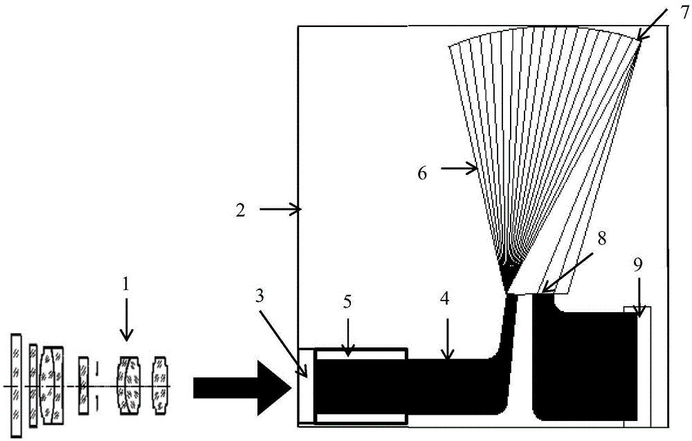
[0064] Such as image 3 It is a schematic diagram of the first embodiment of the present invention, the imaging system 1 images the ground detection area to the slit, and is limited by the slit to obtain a column of light corresponding to 128 pixels coupled into the input waveguide array of the chip, and the coupling loss can be controlled Within 1dB. By controlling the tunable optical attenuator array on the input waveguide, the 128 output waveguide array light intensity signals corresponding to each input channel can be sequentially read, that is, the spectral information of each spatial point.
Embodiment 2
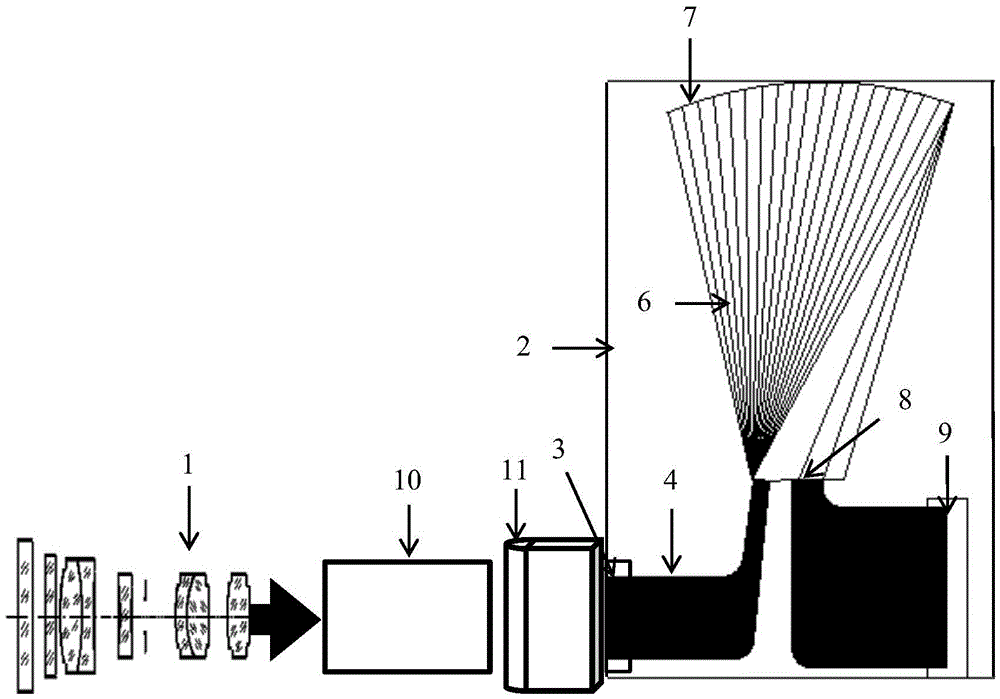
[0066] For the second embodiment, the imaging system is limited by the slit to obtain a row of images corresponding to 128 pixels. The obtained image passes through the optical switch array 10 composed of 128 micromirrors, and then focuses to the taper coupling structure shown in 4 through the cylindrical mirror in the direction perpendicular to the plane of the chip, and finally guides the light into 128 micromirrors such as Figure 5 A large cross-section SOI waveguide is shown. By controlling the optical switch of the micromirror, the switches of different pixels are sequentially turned on, so that only the waveguide corresponding to this pixel has light entering and being split.
[0067] When the imaging spectrometer requires higher spatial resolution, resulting in push-broom imaging requiring more pixels to work in a row, such as 1024 pixels in a row, both embodiments of the present invention can be expanded to 8 above-mentioned spectroscopic systems Evenly distributed o...
PUM
 Abstract
Description
Claims
Application Information