Photocurable and thermocurable resin composition and dry film solder resist
A thermosetting resin, light curing technology, applied in optics, optomechanical equipment, photosensitive materials for optomechanical equipment, etc., can solve the problems of thermal conductivity and electromagnetic absorption performance difficulties, reduce thermal conductivity and other problems, and achieve excellent thermal conductivity and electromagnetic wave absorbing properties, reducing the withstand voltage strength, maintaining the effects of magnetic and thermal conductivity
- Summary
- Abstract
- Description
- Claims
- Application Information
AI Technical Summary
Problems solved by technology
Method used
Image
Examples
Embodiment and
[0215] [Examples and Comparative Examples: Preparation of Resin Composition, Dry Film, and Printed Circuit Board]
Embodiment 1 to 3
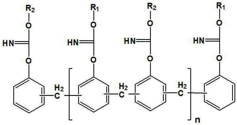
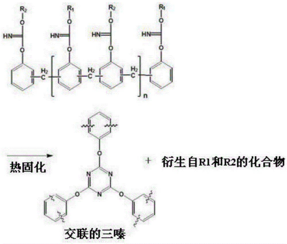
[0217] A bisphenol-based cyanate compound (BA-230) from Lonza was used as the iminocarbonate-based compound of the acid-modified oligomer, and then contained in the bisphenol-based cyanate compound (BA-230) Cyanate groups were reacted with acrylic acid and 1,2,3,6-tetrahydrophthalic acid (4-cyclohexene-1,2-dicarboxylic acid) in a molar ratio of 1:1 to prepare the An aminocarbonate compound which is an acid-modified oligomer.
[0218] Using 45 g of this imino carbonate-based compound, it was mixed with 15 g of ZAR-2000 purchased from NipponKayaku, Co., Ltd. as another acid-modified oligomer, 10 g of ZAR-2000 purchased from SK Cytec Co., Ltd. as a photopolymerizable DPHA of monomer, 2.5g of TPO as photoinitiator, 15g of YDCN-500-80P as thermosetting adhesive purchased from NipponKayaku, Co., Ltd., 0.25g of 2 as thermosetting adhesive catalyst - PI and the inorganic filler described in Table 1 below, 0.3 g of phthalocyanine blue as a pigment, 3.5 g of BYK-110 as a dispersant, an...
experiment Embodiment 1
[0234] Experimental Example 1: Developability (sensitivity) evaluation
[0235] A 12 μm copper foil laminate purchased from Mitsui Mining & Smelting Co., Ltd. was cut into a size of 5 cm × 5 cm, and a good roughness was formed on the surface of the copper foil by chemical etching. After the release film was removed from each dry film prepared in the above examples and comparative examples, the film layer was vacuum laminated with a vacuum laminator (MVLP-500, Meiki Co., Ltd.) to form roughness copper foil laminate (substrate).
[0236] Then, a negative photomask having a hole shape with a diameter of 80 μm was closely adhered thereto, followed by exposing it to UV in a wavelength range of 365 nm at an exposure amount of 350 mJ / cm 2 . Thereafter, the PET film was removed and replaced with 1 wt% Na 2 CO 3 The alkaline solution was developed at 31° C. for a certain period of time, thereby forming a pattern.
[0237] Then, the shape of the pattern formed above was observed ...
PUM
| Property | Measurement | Unit |
|---|---|---|
| glass transition temperature | aaaaa | aaaaa |
| diameter | aaaaa | aaaaa |
| diameter | aaaaa | aaaaa |
Abstract
Description
Claims
Application Information


