

Silicon oxide thin film based low power consumption resistive random access memory and preparation method therefor
A technology of resistive variable memory and silicon dioxide, which is applied in the direction of electrical components, etc., can solve the problems of high operating voltage of resistive variable memory, high preparation temperature of resistive variable layer, and incompatibility of preparation process, so as to save preparation time and cost, and work The effect of low power consumption and power reduction
- Summary
- Abstract
- Description
- Claims
- Application Information
AI Technical Summary
Problems solved by technology
Method used
Image

Examples
Embodiment 1
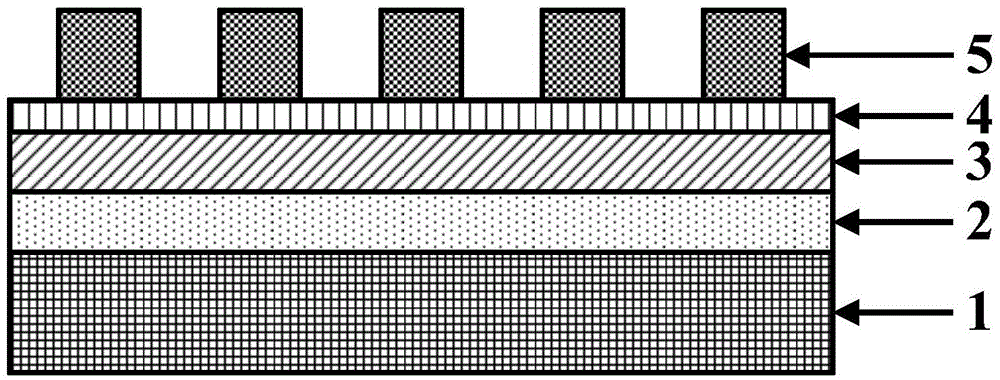
[0036] A low-power resistive memory based on silicon dioxide thin film of the present invention, such as figure 1 As shown, by substrate 1 (silicon is oxidized and the surface generates SiO 2 Silicon wafer with oxide layer, SiO 2 Oxide layer thickness is 200nm), Ti adhesion layer 2 (thickness is 20nm), bottom electrode 3 (100nm thick Pt metal thin film), loose structure silicon dioxide thin film 4 (thickness is 20nm) and top electrode 5 (thickness 50nm dot-like metal Ag thin film) stacked in sequence.
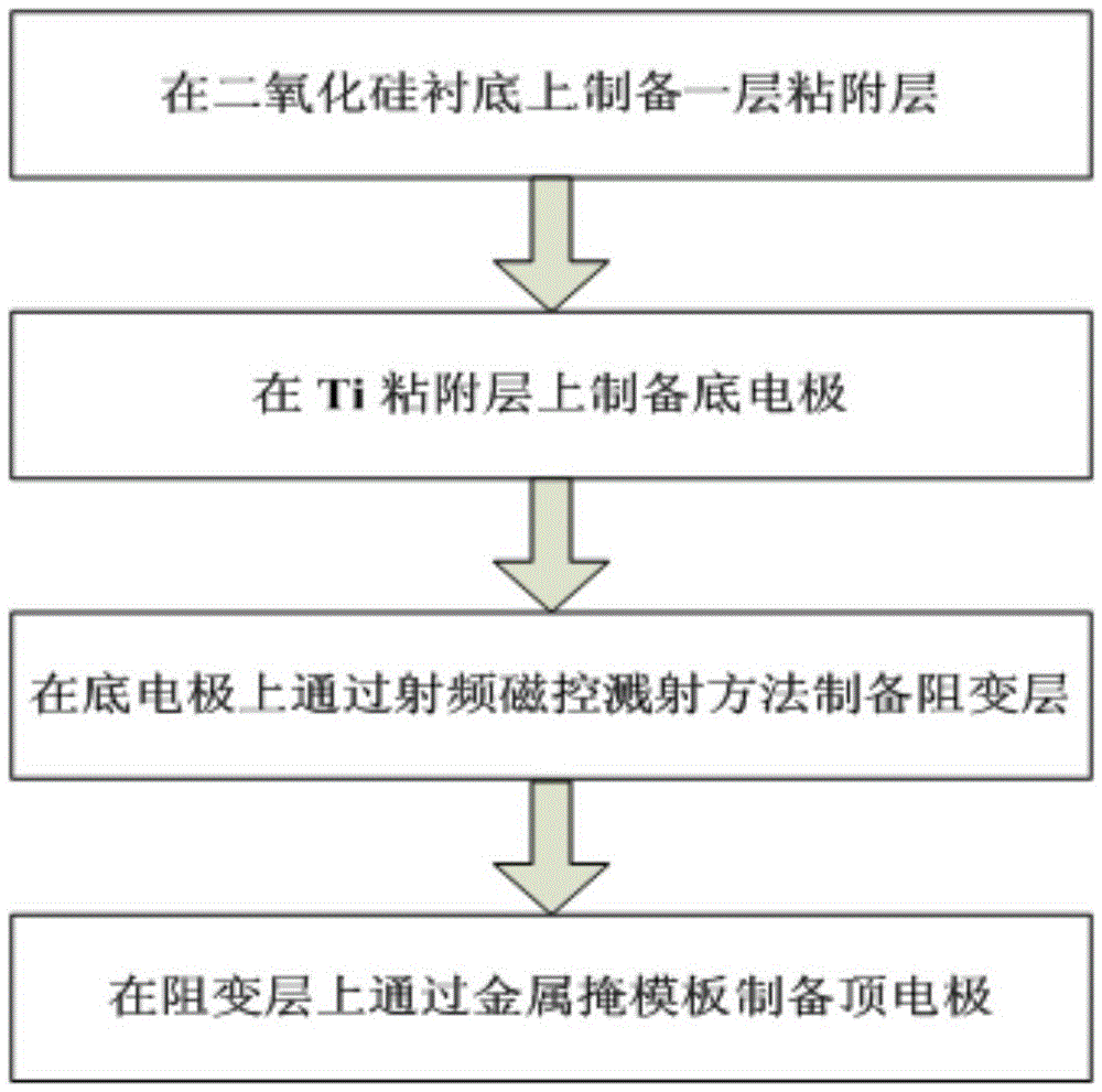
[0037] The preparation method of the silicon dioxide film-based low-power resistive variable memory of this embodiment, its process flow chart is as follows figure 2 shown, including the following steps:
[0038] (1) Prepare a 20nm thick Ti adhesion layer on the substrate by electron beam evaporation;
[0039] (2) Prepare a 100nm thick Pt metal film as the bottom electrode on the Ti adhesion layer by electron beam evaporation;
[0040] (3) On the bottom electrode, prepare a...
Embodiment 2
[0046] A low-power resistive memory based on silicon dioxide thin film of the present invention, such as figure 1 As shown, by substrate 1 (silicon is oxidized and the surface generates SiO 2 Silicon wafer with oxide layer, SiO 2 Oxide layer thickness is 400nm), Ti adhesion layer 2 (thickness is 100nm), bottom electrode 3 (300nm thick Pt metal film), silicon dioxide film 4 (thickness is 40nm) of loose structure and top electrode 5 (thickness 200nm dot-shaped metal Ag thin film) stacked in sequence.
[0047] The preparation method of the silicon dioxide film-based low-power resistive variable memory of this embodiment, its process flow chart is as follows figure 2 shown, including the following steps:
[0048] (1) Prepare a 100nm thick Ti adhesion layer on the substrate by electron beam evaporation;
[0049] (2) Prepare a 300nm thick Pt metal film as the bottom electrode on the Ti adhesion layer by electron beam evaporation method;
[0050] (3) Prepare a 40nm thick silico...
PUM
 Abstract
Description
Claims
Application Information